Quantum physics enables atomic resolution for quantum devices.
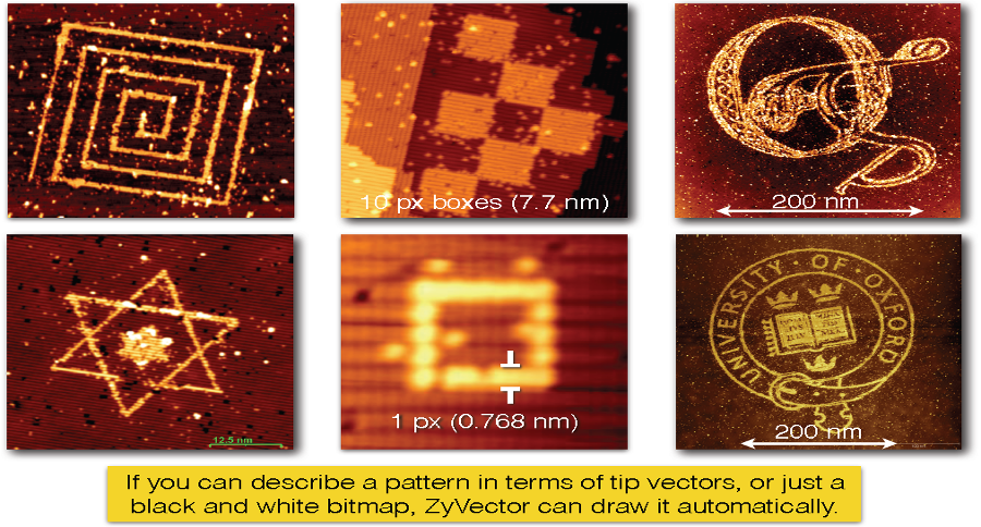
Hydrogen Depassivation Lithography (HDL) is a form of Electron Beam Lithography (EBL) that achieves atomic resolution with very simple instrumentation and uses very low-energy electrons[1]. It uses quantum physics to effectively focus the low-energy electrons and a vibrational heating method to produce a highly non-linear (multi-electron) exposure mechanism. HDL uses a monolayer of H atoms attached to a silicon surface as a very thin resist layer. It uses electron-stimulated desorption to create patterns in the resist. For instance, see the sub-nanometer (nm) exposure exposures below including a 0.768nm line (2 atoms wide) and even individual H atoms removed from the silicon surface.
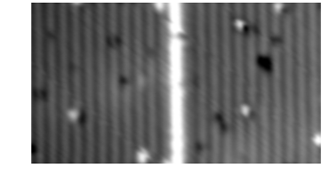
As is shown above on the right, HDL exposures a single H atom spaced on average 0.384nm from other H atoms can be exposed by this technique.
HDL achieves much greater resolution and precision than conventional EBL, which uses large expensive electron-optics systems and very high energy (200Kev) to achieve small spot sizes [2]. But the high-energy electrons (necessary to get small spot sizes) are scattered in the polymeric resist used by conventional EBL and spread the deposited energy creating larger structures as shown in the figure from reference 2.
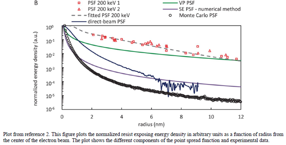
The data shows that the deposited energy in the resist does not drop to 10% of that in the center of the beam until a radial distance of ~4nm.
With HDL we are able to expose single atoms which are >10X smaller than the 10% threshold radius of EBL. This much smaller exposure zone is surprising because HDL uses no optics and simply places a tungsten metal tip approximately 1 nm above the H passivated silicon sample. One would expect that without optics to focus the electrons coming from the tip that the exposure zone would be larger. As suggested by the figure below.
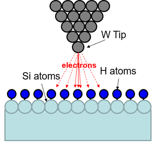
Figure from reference [3] (to scale) showing a W STM tip ~1nm from an H passivated Si surface. It seems unlikely that the electrons would only follow the solid arrow path required to expose a single H atom.
To solve this mystery, we must understand that the electrons are not actually emitted from the tip (in imaging and atomic precision lithography modes) but tunnel from the sample to the tip (in imaging mode) or from the tip to the sample (in lithography mode).
Using a simple model with an infinitely flat and conducting substrate, emission from a single W atom at the apex of the STM tip, and a simplified tunneling current model, we see that the current falls off exponentially with tunneling distance.
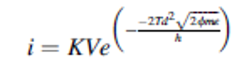
Figure 5 depicts a simple model of HDL. The model assumes an infinitely flat conductor as a substrate and a sphere of radius Rt as the apex of an STM tip. The tunneling current from an STM tip can be modeled with a simplified expression [4]:
where i is the tunneling current, K is a constant, V is the tip to sample bias, Td is the tunnel gap, ɸ is the local barrier height, me is the electron mass, and ħ is Plank’s constant/2π. Using this equation with V = 4 V (a common HDL bias), ɸ = 4 eV (∼the work function of a tungsten tip), and Td = 1 nm, the constant K can be set to 0.194, which would produce a current of 1 nA which is a typical HDL exposure current. A rough rule of thumb for STM tunneling current as a function of tip height is that changing the tip height by ±0.1 nm will decrease/increase the tunnel current by one order of magnitude. Our model predicts a decrease/increase by a factor of 7.75, lending some credibility to the model.
Using this model, we can predict the radial distribution of the tunneling current on the sample as shown in the following figure:
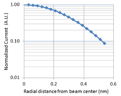
However, this alone does not explain the atomic resolution of HDL. With H atoms only separated by 0.384nm, even with perfect tip positioning and a stochastic (quantum) exposure mechanism, we would expect to see an error rate (neighboring H atoms removed) about 30% of the time.
However, at a bias of 4V, there is sufficient energy transfer by a single electron impact, and HDL in the atomic resolution mode is a highly non-linear exposure process where the exposure probability varies with the 5th order of tunneling current.
When the dependence on the current is applied to the current distribution there is a significant sharpening of the exposure efficiency as shown in the figure below:
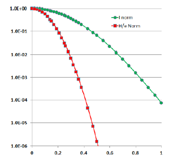
Figure[3] shows the normalized current distribution due to the quantum tunneling effect and the normalized exposure efficiency Hydrogen atoms are desorbed per electron as a function of radial distance (in nm) from the peak.
For the usual mode of exposing patterns with HDL, the lateral distance to an unwanted exposure is ~0.47nm leading to an error rate of 10-6.
For solid-state quantum devices where energy levels and tunneling rates are extremely sensitive to variations in distance, HDL is the ideal choice for solid-state quantum device manufacturing.
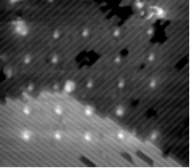
Several examples of HDL Lithography are shown below:
References
- Randall, J. N., Owen, J. H. G., Lake, J., & Fuchs, E. (2019). Next generation of extreme-resolution electron beam lithography. Journal of Vacuum Science & Technology B, 37(6), 061605. https://doi.org/10.1116/1.5119392
- Manfrinato, V. R., Wen, J., Zhang, L., Yang, Y., Hobbs, R. G., Baker, B., Su, D., Zakharov, D., Zaluzec, N. J., Miller, D. J., Stach, E. A., & Berggren, K. K. (2014). Determining the resolution limits of electron-beam lithography: Direct measurement of the point-spread function. Nano Letters, 14(8), 4406–4412. https://doi.org/10.1021/nl5013773
- Randall, J. N., Owen, J. H., Fuchs, E., Saini, R., Santini, R., & Moheimani, S. O. R. (2020). Atomically precise digital e-beam lithography. In E. M. Panning & M. I. Sanchez (Eds.), Novel Patterning Technologies for Semiconductors, MEMS/NEMS and MOEMS 2020 (Issue March 2020, p. 31). SPIE. https://doi.org/10.1117/12.2552083
- See: http://www2.fkf.mpg.de/ga/research/stmtutor/stmtheo.html.