ZyvexLitho1™
A complete Scanning Tunneling Lithography System with features not available on any other commercial Scanning Tunneling Lithography System.
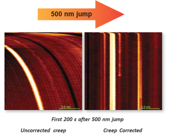
Distortion Free Imaging:
Our proprietary Creep and Hysteresis Correction algorithm permits distortion free imaging and atomically precise tip positioning for unprecedented accuracy in lithography.
Adaptable Current Feedback Loop:
All commercial STMs use the same Proportional Integrating (PI) loop to raise and lower the STM tip as it scans to maintain a set point current. Unfortunately, with this simple control loop tip crashes are a common occurrence. This can be tolerated if you are simply imaging but is a serious problem when doing lithography. A patented adaptable current control loop is incorporated into ZyvexLitho1’s control system that dramatically reduces tip crashes.
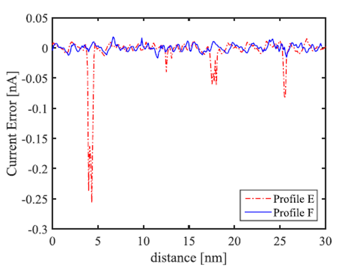
The Figure shows a line scan across a Si surface where there are several perturbations that cause a current error in profile E where the control loop is a standard PI loop. In profile F the adaptable control loop is turned on and the tip scans over the same line. The more accurate current control provides a more accurate profile and when surface perturbations are larger, avoids tip crashes. From: Tajaddodianfar, F., Moheimani, S. O. R., & Randall, J. N. (2018). Scanning Tunneling Microscope Control: A Self-Tuning PI Controller Based on Online Local Barrier Height Estimation*. IEEE Transactions on Control Systems Technology, 1–12. https://doi.org/10.1109/TCST.2018.2844781
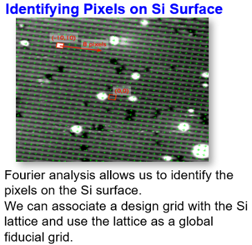
Automatic Lattice Alignment:
Because the lithography modes and imaging modes are well separated in energy, the Si surface can be imaged before and after lithography. This non-exposing imaging mode permits the automated identification of the Si lattice and therefore the position of the pixels on the surface. This Lattice Lock process automatically keeps the tip positioning (and therefore the lithography) accurate.
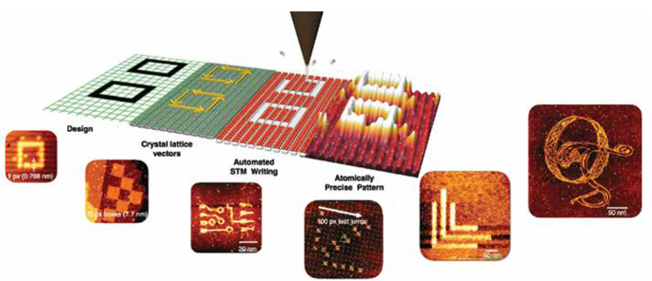
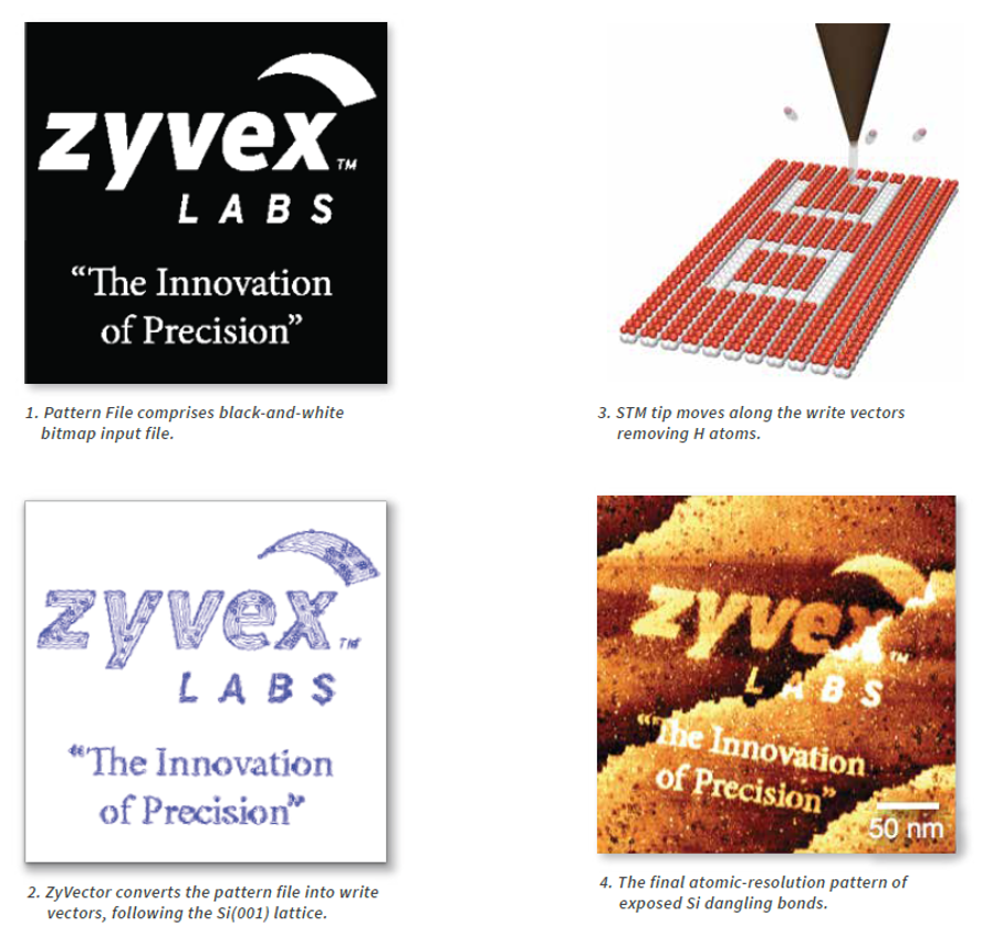
Digital Vector Lithography
ZyvexLitho1 uses Hydrogen Depassivation Lithography to remove H atoms from a Si (100) 2×1 reconstructed surface. This self-developing exposure technique is binary in nature. Either the H-Si bond is broken (sending the H atom into the vacuum) or it is not. There are no partial exposures or proximity effects. Making use of this process and the global fiducial grid that is the Si surface lattice permits Digital Lithography. The sub-nm pixel is 4 surface Si atoms. Computer Aided Design (CAD) files where the design grid is the same as our pixel grid may be loaded into ZyvexLitho1 and the pattern may be automatically fractured into different geometries allowing tip vectors to be used with different lithography modes. Exposures can then be carried out automatically.
Automation and Scripting:
Almost all actions can be automated. Command-line interface for single commands or scripts. Script Menu for built-in and user-written scripts. Multiple pattern input modes – as geometric shapes, vector lists, black/white bitmaps.
Built-in Metrology:
A non-destructive imaging mode is available so that new patterning can be aligned to the old and pattern quality can be checked after writing.