How to make a P-in-Si quantum device
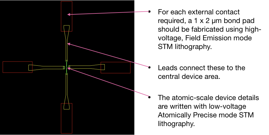
We wish to lower the technical barriers facing scientists wanting to explore atomic-scale devices. As shown schematically below, the process of creating buried-dopant devices involves a significant number of steps. First, the device to be fabricated needs to be designed, from the atomic-scale device components up to the bond pads to connect to the outside world. A substrate with prepatterned alignment marks to allow the device to be located after burial should be created, and prepared in UHV for STM patterning. The device pattern is then created using atomically-precise Hydrogen Depassivation Lithography (HDL). Phosphine (PH3) or another dopant precursor is adsorbed into the pattern and incorporated, and then the pattern is buried in epitaxial silicon to a depth of 20 nm or more. After this, the device chip can be removed from vacuum, the buried device located relative to the alignment marks so that contacts can be made, wiring added, and then the device is ready for testing and measurement of its properties, typically in a cryostat or dilution fridge.
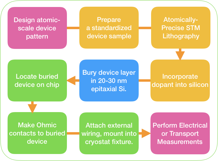
Design atomic-scale pattern
Make a H-terminated device sample with alignment marks
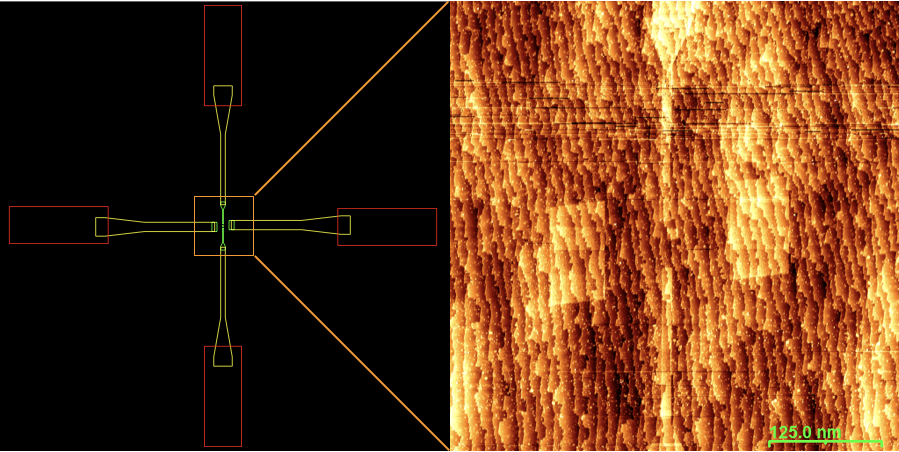
Atomically-Precise STM Lithography
Incorporate Dopant
From:
Fuechsle et al. Nat Nano 7 242-246 (2012) DOI: 10.1038/nnano.2012.21
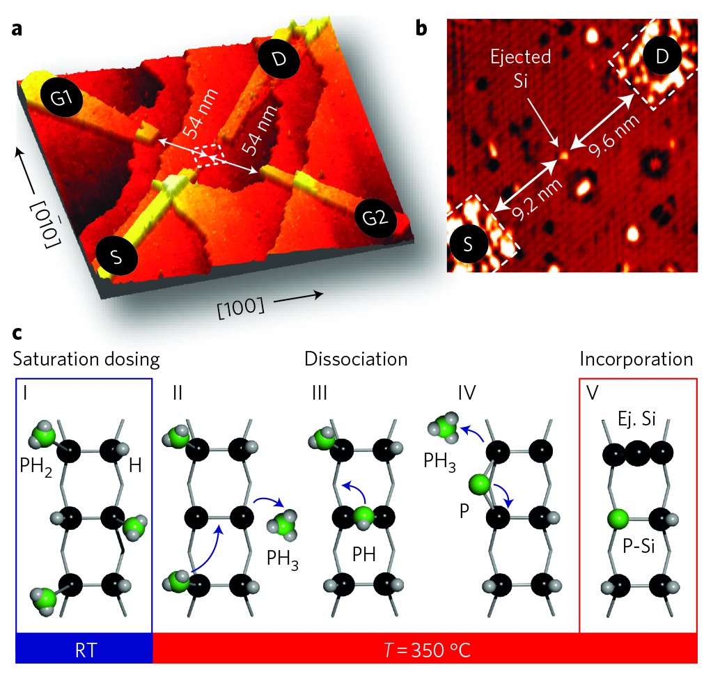
The STM-defined patterns are filled with phosphine (PH3) gas. An incorporation anneal for 1-2 min. at 380°C drives a surface chemical process during which some of the PH3 leaves the surface, and the remainder loses H, and then the P atom exchanges with a Si dimer atom.
The amount of incorporated P can therefore be judged from the amount of ejected Si.
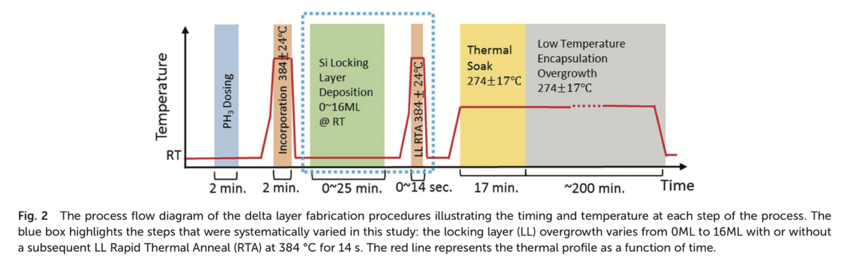
Device Burial in 20nm epitaxial Silicon
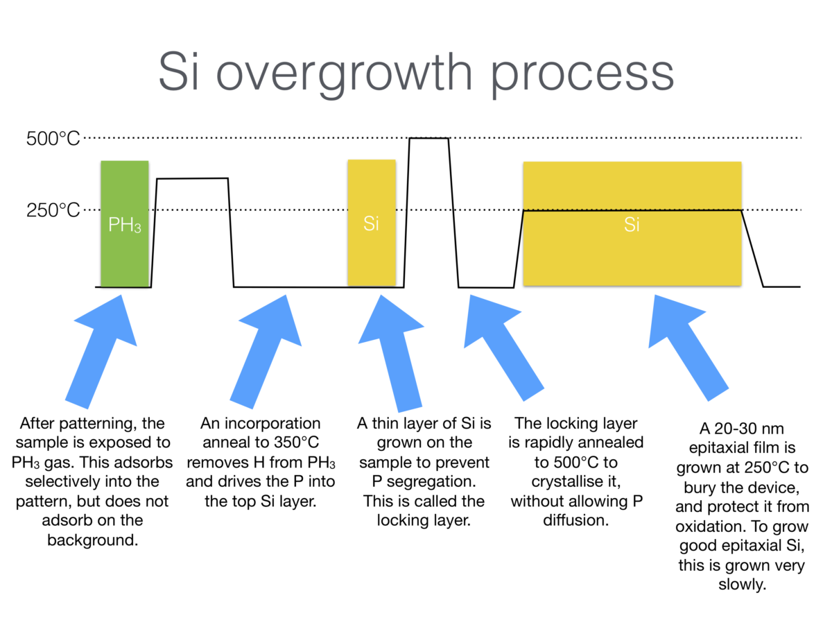
The incorporated P needs to be buried, both to protect it from atmospheric oxidation, and also to separate the dopant states electrically from surface states, and other electronic impurities which would destroy the device properties.
In order to prevent segregation of the P up to the surface during overgrowth, a locking layer is first deposited with the substrate at room temperature. This locking layer will be amorphous, and is then annealed to recrystallise it. After that, the overgrowth proceeds, keeping the overall temperature low to prevent diffusion of the dopant atoms during overgrowth. This low temperature requires slow growth, to maintain good crystallinity. Typically, 270°C is used for overgrowth.
The figure below comes from a detailed discussion of the burial process, which can be found at: X. Wang et al. Nanoscale 10, 4488 (2018). DOI: 10.1039/C7NR07777G
Locate buried device on chip
Despite being buried under 20 nm of Si, the electronic states of the device can still be detected using dI/dV imaging. A small amplitude is applied to the sample bias, and differences in the tunnel current are detected using a lock-in amplifier. The large scale parts of the devices, such as wires and bond pads can then be detected using the STM tip. The device location is then identified relative to surface alignment marks, so that subsequent processing, such as adding electrical contacts, will place surface contacts in the right place.
Attach Ohmic contacts to buried device
In order to perform electrical measurements, electrical contacts must be made to the buried device. One way to do this, is to lay down Al contacts on the surface, and anneal, so that the Al diffuses down through the delta layer, making an Ohmic contact. Similarly, Pt or Pd can be deposited, which then forms a silicide which penetrates down to the delta layer.
Perform electrical measurements
With the sample now complete, the device chip can be mounted into the measurement insert, and transferred into a dilution fridge for electrical measurements.
Bibliography
[1] F. J. Ruess, L. Oberbeck, K. E. J. Goh, M. J. Butcher, E. Gauja, A. R. Hamilton, M. Y. Simmons, and F. J. Rue ss, Nanotechnology 16, 2446 (2005).
[2] T. Hallam, T. C. G. Reusch, L. Oberbeck, N. J. Curson, and M. Y. Simmons, J. Appl. Phys. 101, 34305 (2007).
[3] J. N. Randall, J. W. Lyding, S. Schmucker, J. R. Von Ehr, J. Ballard, R. Saini, H. Xu, and Y. Ding, J. Vac. Sci. Technol. B 27, 2764 (2009).
[4] A. Fuhrer, M. Füchsle, T. C. G. Reusch, B. Weber, and M. Y. Simmons, Nano Lett. 9, 707 (2009).
[5] B. Weber, S. Mahapatra, H. Ryu, S. Lee, A. Fuhrer, T. C. G. Reusch, D. L. Thompson, W. C. T. Lee, G. Klimeck, L. C. L. Hollenberg, and M. Y. Simmons, Science (80-. ). 335, 64 (2012).
[6] E. Bussmann, M. Rudolph, G. S. Subramania, S. Misra, S. M. Carr, E. Langlois, J. Dominguez, T. Pluym, M. P. Lilly, and M. S. Carroll, Nanotechnology 26, 6 (2015).
[7] M. Y. Simmons, IEDM 9, 1 (2015).
[8] X. Deng, P. Namboodiri, K. Li, X. Wang, G. Stan, A. F. Myers, X. Cheng, T. Li, and R. M. Silver, Appl. Surf. Sci. 378, 301 (2016).
[9] D. R. Ward, M. T. Marshall, D. M. Campbell, T.-M. Lu, J. C. Koepke, D. A. Scrymgeour, E. Bussmann, and S. Misra, 87185, 1 (2017).
[10] T. Škereň, N. Pascher, A. Garnier, P. Reynaud, E. Rolland, A. Thuaire, D. Widmer, X. Jehl, and A. Fuhrer, Nanotechnology 29, 435302 (2018).
[11] X. Wang, J. A. Hagmann, P. Namboodiri, J. Wyrick, K. Li, R. E. Murray, A. Myers, F. Misenkosen, M. D. Stewart, C. A. Richter, and R. M. Silver, Nanoscale 10, 4488 (2018).