Digital Vector Lithography
Unlike conventional optical or e-beam lithography, STM lithography takes into account the atomic nature of the surface. In ZyVector, writing is done as vectors, moving along the surface lattice directions, rather than a raster scan across the surface as used for STM imaging.
Hydrogen Depassivation Lithography (HDL)
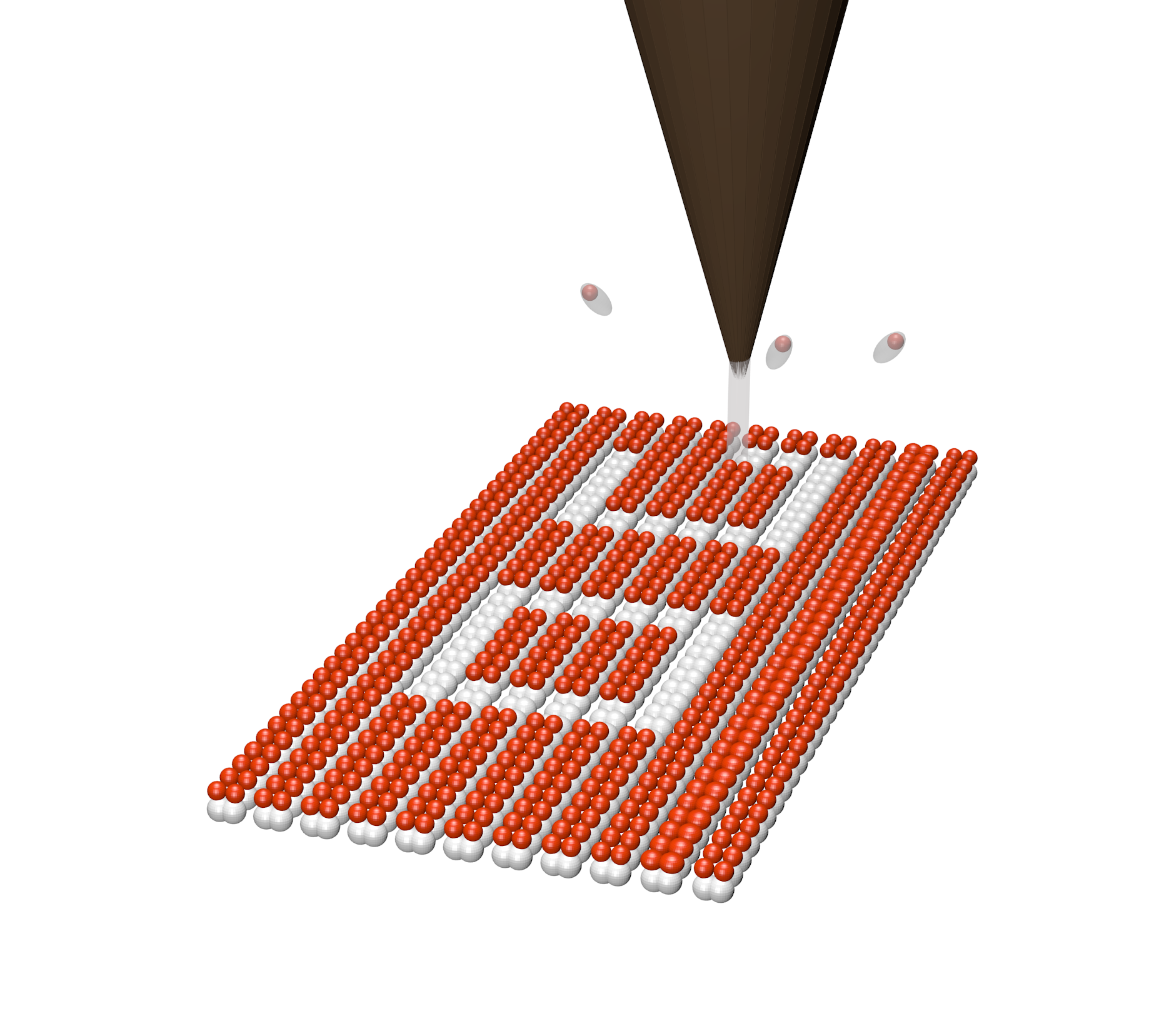
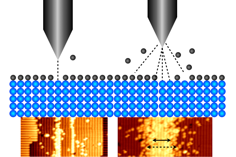
Lyding et al.* first showed that at a positive sample bias, an STM tip can be used to inject electrons into a surface Si-H bond, until the bond breaks, exposing a chemically reactive Si dangling bond. Other materials are then selectively reacted with the dangling bonds, forming atomically precise nanostructures.
*Applied Physics Letters 64 2010-2012 (1994)
Atomic-scale Lithography Pixel
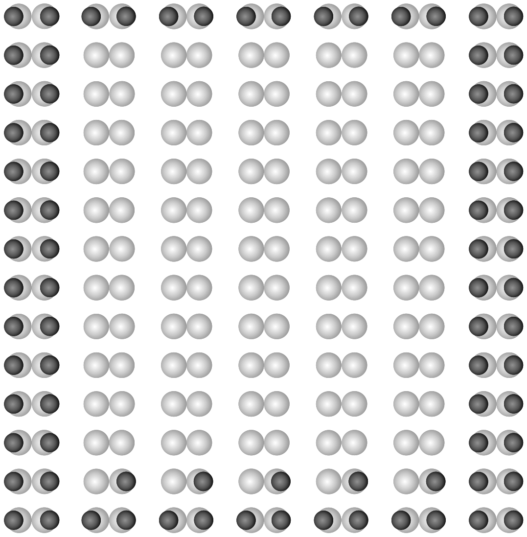
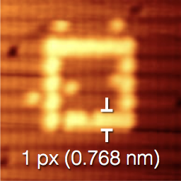
For the Si(001):H surface, we use a standard pixel size of 2 dimers on a single dimer row, giving a lithography pixel size of 0.768 nm. Patterns are typically generated from integral numbers of pixels, although for some special cases, such as the 3-dimer pattern used to place single phosphorus dopant atoms, half-pixels can also be used.
![]()
Writing to the Lattice
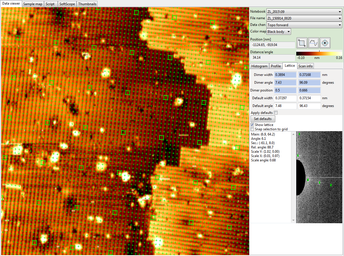
In order to write atomically-precise patterns, the location of the surface dimer rows is identified from the Fourier Transform of an STM image, and a pixel grid is overlaid onto the image.
To perform lithography, the tip is then instructed to move to a particular pixel, change to lithography conditions and write a line along or across the dimer rows of the desired length.
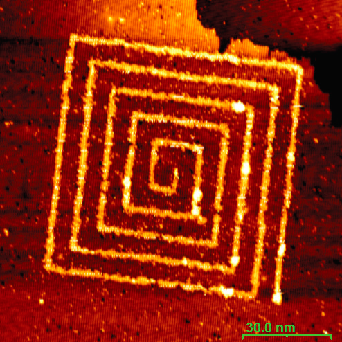
Variable Spotsize Lithography
STM lithography is digital because it causes the breaking of a Si-H chemical bond by electron excitation. There is no equivalent of partial exposure, because either the bond is broken or it is not. Likewise, there are no proximity effects.
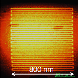
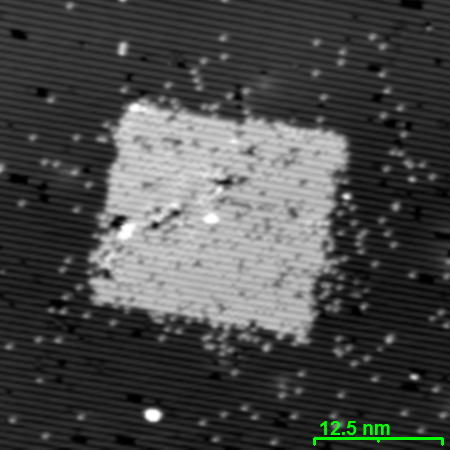
Similar to e-beam lithography, with different settings of bias voltage and tunnel current, multiple line widths areavailable, from 1 px width up to several nm. Under low-voltage lithography conditions, around +4 V, 4 nA, with a dose of 4 mC/cm, the line width of STM lithography is one dimer row. This is known as Atomically Precise or AP mode. Above about 6 V, the tip moves out of tunneling range into Field Emission (FE) mode with much wider line widths, but also with rough edges to the lines. Use of the FE mode is useful to minimize write time for larger patterns, particularly where there is less need for absolute precision. For large patterns which do require precise edges, the modes can even be mixed within a single pattern, writing slowly around the perimeter, and quickly filling in the centre.
Writing Simple Patterns
Simple shapes can be selected in the Litho Pattern tab and written with just one or two clicks.
In the Script Menu tab, geometric patterns can also be called, with editable parameters, such as dimensions and angles. Here, alignment to the lattice can be turned on and off as required.
Current, voltage and electron dose parameters are selected in the Litho tab. Preset groups of parameters giving different linewidths can be saved, and quickly selected.
Removing single atoms
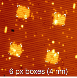
For removal of single H atoms, or single dimers, Feedback Controlled Lithography (FCL) is more reliable than simply drawing a very short line.
The Litho trap settings in the Litho tab allow for the litho mode to be exited immediately when a sharp change in the tunnel current, or other trigger, is registered.
This sharp change indicates the removal of one or two H atoms under the tip. Single dots, lines or arrays of single dimer patterns can be produced using scripts incorporating Feedback Controlled Lithography.