The idea of Atomically Precise Manufacturing (APM) comes from Richard Feynmann's famous speech, “Plenty of Room at the bottom” in which he predicted that one day we would be able to build structures atom by atom. Our founder, Jim Von Ehr, started Zyvex with the express purpose of developing Atomically Precise Manufacturing. Instead of continuing to improve manufacturing precision, we are beginning to realize atomic precision by taking advantage of the fact that matter is made up of atoms and molecules.
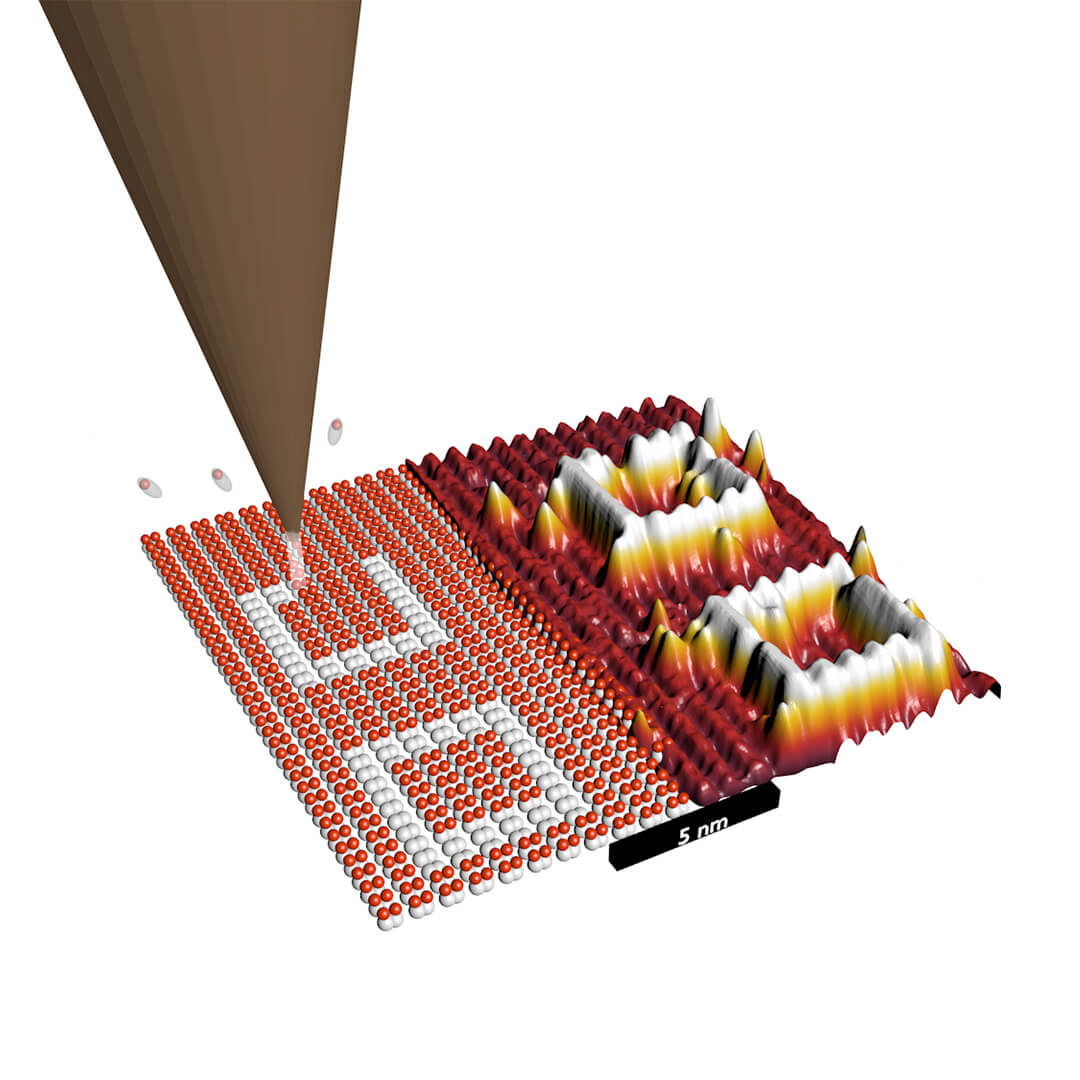
While there are many approaches to atomically precise manufacturing, we focus on creating patterns with a resolution down to a single atom with a process called hydrogen depassivation lithography (HDL). HDL was first demonstrated by Prof. Joe Lyding of University of Illinois at Urbana-Champaign in 1994. He showed that the tip of a scanning tunneling microscope (STM) could be used to inject electrons into surface chemical bonds, causing them to break. In particular, this process allowed single hydrogen atoms to be removed from a silicon surface. By scanning the tip across the surface at suitable voltage and current conditions, lines of hydrogen atoms can be removed, creating patterns of exposed silicon dangling bonds, which are more reactive to many species than the hydrogen-terminated silicon atoms, thus producing chemical contrast.
Due to this strong chemical contrast, many different species prefer to adsorb into the patterned areas and do not stick onto the hydrogen-terminated background. Over many years, different species have been tested by various research groups, from metals such as aluminum, gallium, indium and silver, to simple molecules such as ammonia, hydrocarbon molecules, (e.g. norboradiene) and metal precursors (e.g. trimethyl aluminium).
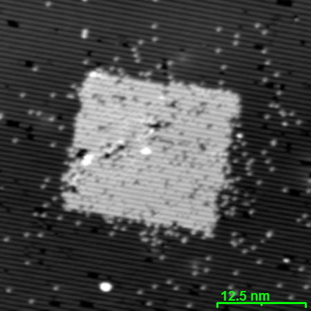
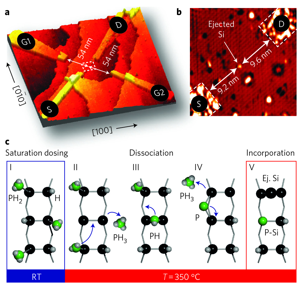
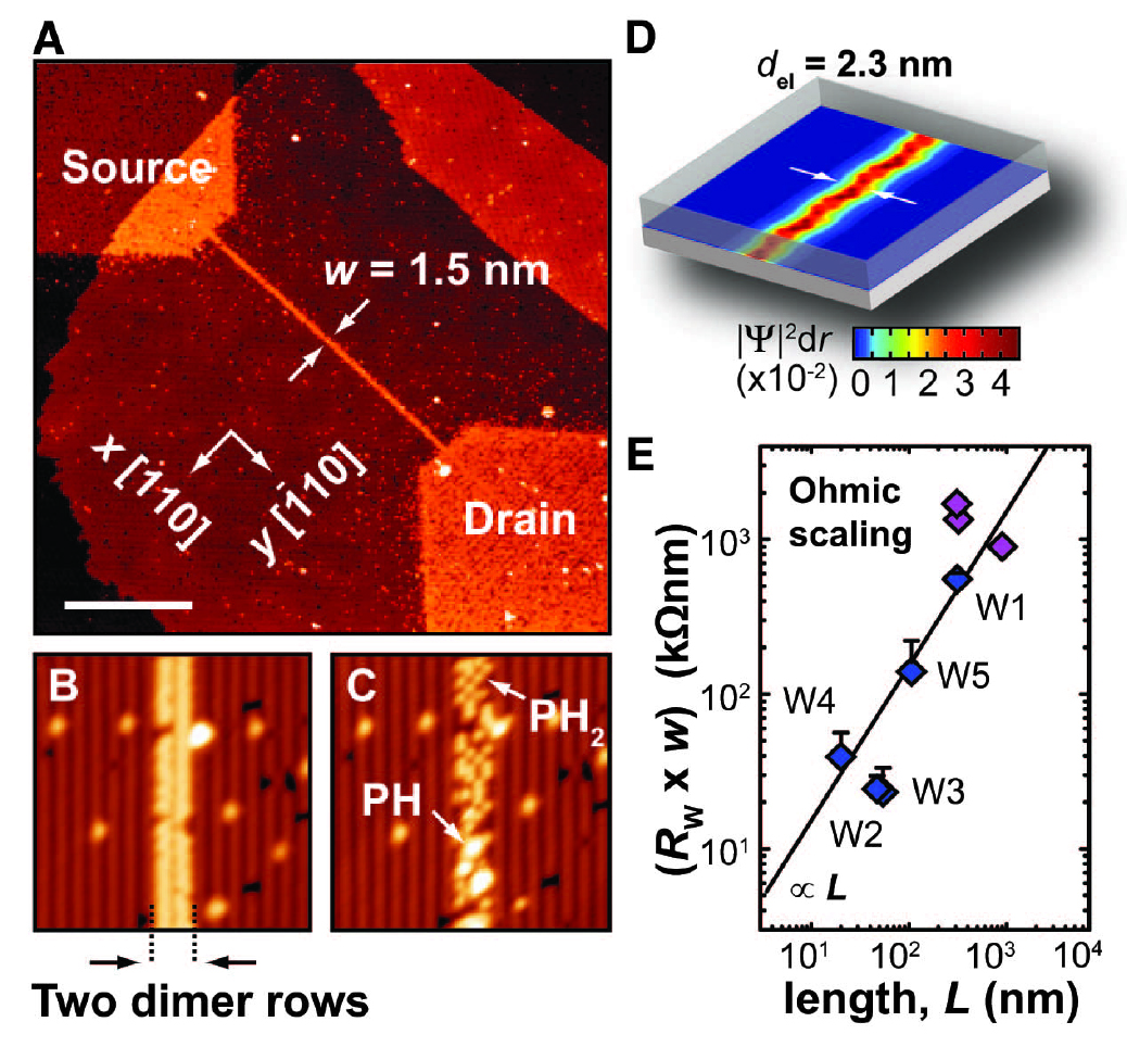
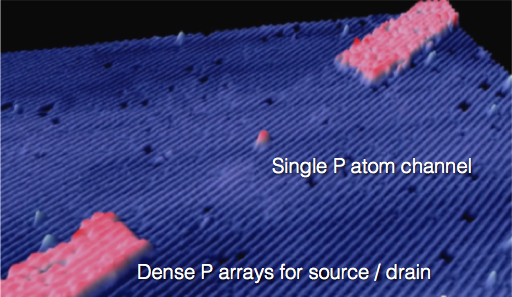
Recently, the first practical application of HDL was developed at the University of New South Wales (UNSW), Australia. Researchers created nanoscale electronic devices, including wires, transistors and quantum dots (e.g. interconnects and um-scale bond pads) to connect to the outside world. The HDL patterns were filled with phosphine and, using a short anneal, the phosphorous atoms were incorporated as dopants into the silicon, thus creating metallic conductors, electrodes, gates, and even the ‘single-atom transistor,’ where one isolated phosphorus dopant forms the channel of the transistor.
Positioning of single dopant atoms is a promising route to creating a quantum computer, in which the digital bits of a classical computer are replaced with quantum bits, or qubits. This would allow certain classes of problems, such as cryptography, to be calculated much faster than what is currently possible with classical computer technology. Single phosphorus atoms have established advantages for quantum computing, including single-electron and nuclear spin-1/2 states with exceptionally long coherence times situated in the industrially-relevant silicon platform. Proposals for silicon:phosphorus donor-based quantum computing architectures are all founded on a regular periodic array of phosphorus donors at a nanoscale pitch. Atomic-precision phosphorus placement via scanning tunneling microscopy (STM) and hydrogen depassivation lithography (HDL) mitigates the stochastic spatial scatter, inherent to more conventional ion implant techniques, that is predicted to have severe impacts on 2-donor-gate interactions. To scale these devices up from 1 to 2, to 4 or even 10 qubit devices, tools for patterning with atomic precision, with high reliability and throughput, are required.