ELECTRON OPTICS
Definition: Focusing and deflecting electron beams using assembled MEMS lens elements.
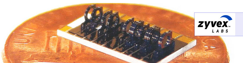
An early test showing precision assembly of an Einzel lens on a silicon substrate. Zyvex Labs’ assembly technology allows submicron precision for the size, shape, and spacing of each lens element. The snap connector sockets on the base also allow electrical connection to assembled components. |
 |
|
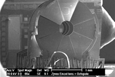
Closeup of an octopole lens element. A broken contact at the base allowed the topmost segment to electrically float, so it charged up in the SEM, appearing brighter in this image. |
 |
|
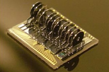
Optical closeup of the completed mini-SEM lens assembly. Typical precision of these lens elements is within 1/2 degree of vertical without any glue at the base, but becomes much better when the lens elements are glued in after assembly. Such glued joints have been tested to withstand well over 15000 G's - the silicon parts break before the glued joints. This prototype supported several hundred volts across the lens elements, limited by substrate breakdown. A different substrate would allow thousands of volts between lens elements. |
|
|
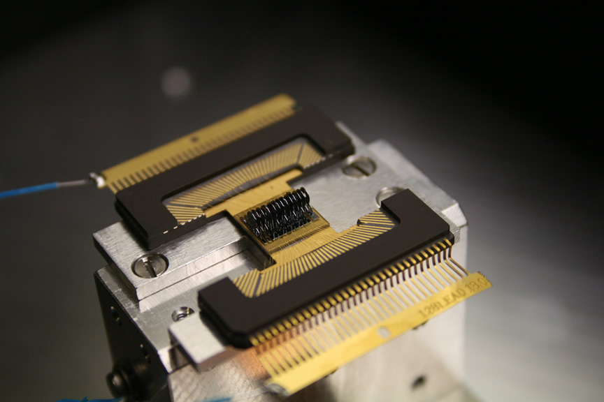
Optical closeup of the packaged lens assembly. Click to see a larger image of this. |
 |
|
© Copyright 2015. Zyvex Labs, LLC.