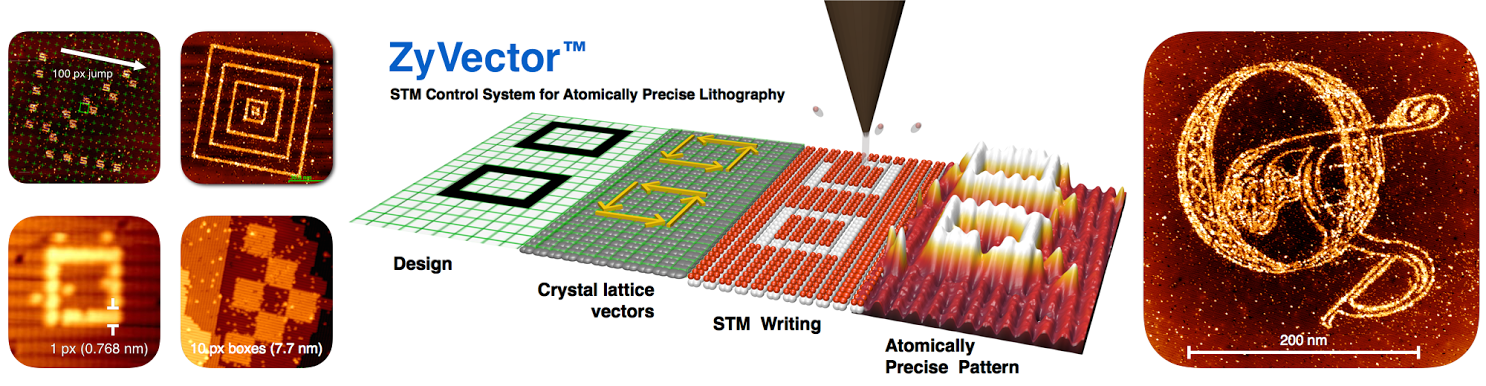
ZyVector TM | STM LITHOGRAPHY CONTROL SYSTEM
Our system contains all of the necessary outputs and software to apply/read voltages to/from:
- 4 fine x/y channels
- 1 fine z channel
- 3 coarse XYZ channels
- 1 tip bias channel
- pre-amp gain control
- pre-amp bias control
- amplified current input
With these controls the user should be able — assuming adequate tip/sample/system quality — to perform STM scanning and HDL of complex patterns.
We expect the following functionality:
- Walk-in
- Fast walk-in. This mode is where the coarse ramp rate is kept too high (50,000 nm/s) for effective tunneling detection. This is performed under optical feedback.
- Automated walk-in. This mode is just like Fast walk-in, except it is performed with a slower tip ramp rate (on order of 1000-2000 nm/s) and a high (~-9V tip) voltage. When a current is detected, the coarse piezo freezes and the fine piezo retracts from the surface a specified amount. Feedback is otherwise “on” here.
- Engage. This mode uses scanning conditions to bring the tip into contact with the sample. This is a very slow Automated walk-in followed by a “homing” process.
- Tip stepping
- We can move the tip sideways in x/y, using coarse piezos with the tip retracted from the surface a safe distance.
- Scanning
- Scanning of the surface with any size from 1-10,000 nm in x/y with rectangular scan aspect ratios available.
- Minimum scan pixel grid defined as 135V*calibration(nm/V)/216/division.
- division selectable between 1, 4, 14.
- (alternately: nominal scan range determined as 135V*calibration(nm/V)/division)
- Fast scan direction arbitrarily defined between 0 and 359.9 degrees relative to piezo tube axes.
- Many other scan controls available, as established in SCANZ.
- HDL
- Two modes possible
- AP mode
- FE mode
- Three input modes
- Bitmap input with each bitmap pixel correlating to a surface pixel of two dimers.
- Lattice pattern input with tip following a lattice registered path
- Litho pattern input independent of lattice if necessary (i.e., not necessarily a “Manhattan geometry” approach.)
- Advanced position controls (assuming adequate sample and tip condition)
- Piezo tube calibration based on lattice recognition, at least over the central portion of the scan range.
- Including determination of lattice angle relative to piezo tube axis.
- Linear creep correction in x/y
- Initial optimization of creep over timescales of 0.1s – 3600s
- Optimized over central portion of scan range, applied over entire piezo-tube range
- Lattice phase recognition
- Scripting capabilities
- We will provide scripts for test HDL patterns as well as additional scripts for basic functions and basic device patterns.
- Additional image and data archiving and analysis tools.
Distributed by
![]()
For more information, please contact info@zyvexlabs.com.
© Copyright 2015. Zyvex Labs, LLC.