APMC APPROACH TO ATOMICALLY PRECISE MANUFACTURING (APM)
This work has been supported by research contracts from DARPA (Feasibility of Atomically Precise Manufacturing, program ID HR0011-07-0049 and Atomically Precise Manufacturing, program ID N66001-08-C-2040) and the State of Texas' Emerging Technology Fund.
Our work is done in a custom-built UHV chamber, using a custom-built STM modeled on the Lyding design, running custom software we developed.
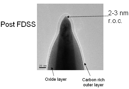
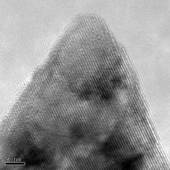
1) In an Ultra-High-Vacuum chamber, use a sharp tungsten tip... A sharp STM tip — approximately 2nm radius of curvature on end. The image on the left shows oxide and carbon contamination due to handling in air and TEM imaging after preparation. The image on the right is a high-resolution TEM image showing the tungsten atomic lattice at the end of the tip. We are investigating use of a single-atom tip to achieve even higher resolution. |
||
 |
||
 |
||
|
||
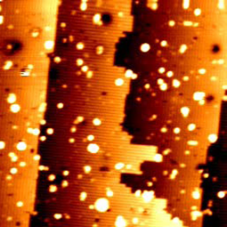
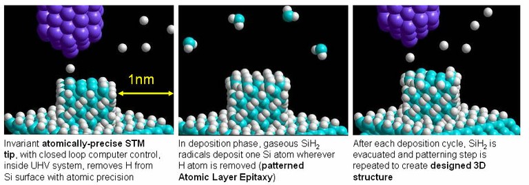
2) ...on a hydrogen-passivated Typical hydrogen passivated silicon <100> surface, showing 2x1 reconstruction and surface contamination. Each of the rows represents a dimer of silicon — a higher magnification image would show pairs of atoms crosswise to the major direction of the dimer. Surface preparation is important, and much better surface quality is possible, but our priority right now is better precision and more reliable lithography. This surface shows numerous missing atoms and contaminants scattered about the surface, but these do not currently interfere significantly with our lithography development. |
 |
|
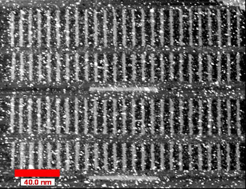
3) ...to pop off the hydrogen and perform atomic-precision lithography. 100 lines of silicon depassivation with better than +- 10% control over length. Some imprecision in the lines is due to piezo creep and hysteresis during the several minutes this took to write. Work is underway to correct for some of these effects.
|
 |
|
| 4) Then grow on the depassivated region via a self-limiting deposition process, and repeat. | ||
 |
||
5) Make valuable products with atomic precision, including massively parallel versions of the lithography-based manufacturing hardware, which can then make greater quantities of atomically precise products less expensively, leading to still better manufacturing hardware... This results in a double-declining learning curve: as we get better at manufacturing products less expensively, the factory itself will also become better and less expensive. This contrasts with the semiconductor industry, where wafer fabs become geometrically more expensive with each new generation of technology. |
||
This approach to nanotechnology leads to Productive Nanosystems. Zyvex Labs actively participated in developing the 2007 Technology Roadmap for Productive Nanosystems, jointly published by Battelle and the Foresight Institute, with financial support from the Waitt Family Foundation. |
 |
|
© Copyright 2015. Zyvex Labs, LLC.