←2009 |
2011→ |
MNE 2010 Micro Nano Graph Contest
“ A good Micrograph is worth more than the MegaByte it consumes.”Entries Presented by Dr. John Randall – Zyvex Labs
Sponsored by
The rules include the following:
• Entries have to be of a single image taken with a microscope and not significantly altered.
• There is no restriction with respect to the subject matter.
• Electron and ion micrographs have to be black and white.
In 2010, 60 entries were submitted. There were many outstanding micrographs. The work represented in the submitted micrographs covered a wide range of fields including micro mechanical, photonic, and integrated circuit fabrication, chemical and dry etching, laser optics, carbon nanotube structures, carbon nanotube growth experiments, biological samples, material science experiments and, of course, e-beam, ion beam, and nano imprint lithography experiments.
The panel of judges who selected the award winners were:
- Cinzia Paglia – Italy
• Massimo De Vittorio – Italy
• Evangelos Gogolides – Greece
The Awards are:
• First Prize
• Second Prize
• Third Prize
The judges also selected 6 Honorable Mentions.
All 2010 Entries (with original titles)
Judges exercised their prerogative to change the micrograph titles if it pleased them.
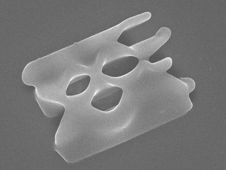
First Prize
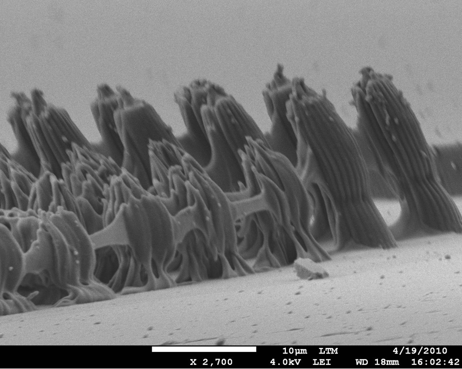
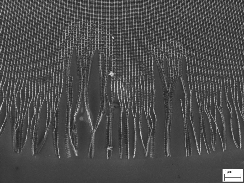
Title: “March of the penguins” “ La Marcia dei Pinguini ”
Description:
2-photon polymerization (TPP) of Poly-Ethylene-Glycol (PEG). Exposition conditions (voxel size – overlap – TPP dose) are not well controled.
Magnification (3″x4″ image): 2.7K X
Instrument: Zeiss Ultra PLus
Submitted by: Thibault Honegger
Affiliation: LTM-CNRS, CEA
Second Prize

Title: “Louisiana coast”
Description:
A defect in the imprint mask caused SU-8 resist to spread all over the sample.
Magnification (3″x4″ image): 905 X
Instrument: Carl Zeiss, Supra 55VP
Submitted by: Birgit Päivänranta Arne Schleunitz
Affiliation: Paul Scherrer Institut Villigen, Switzerland
Third Prize
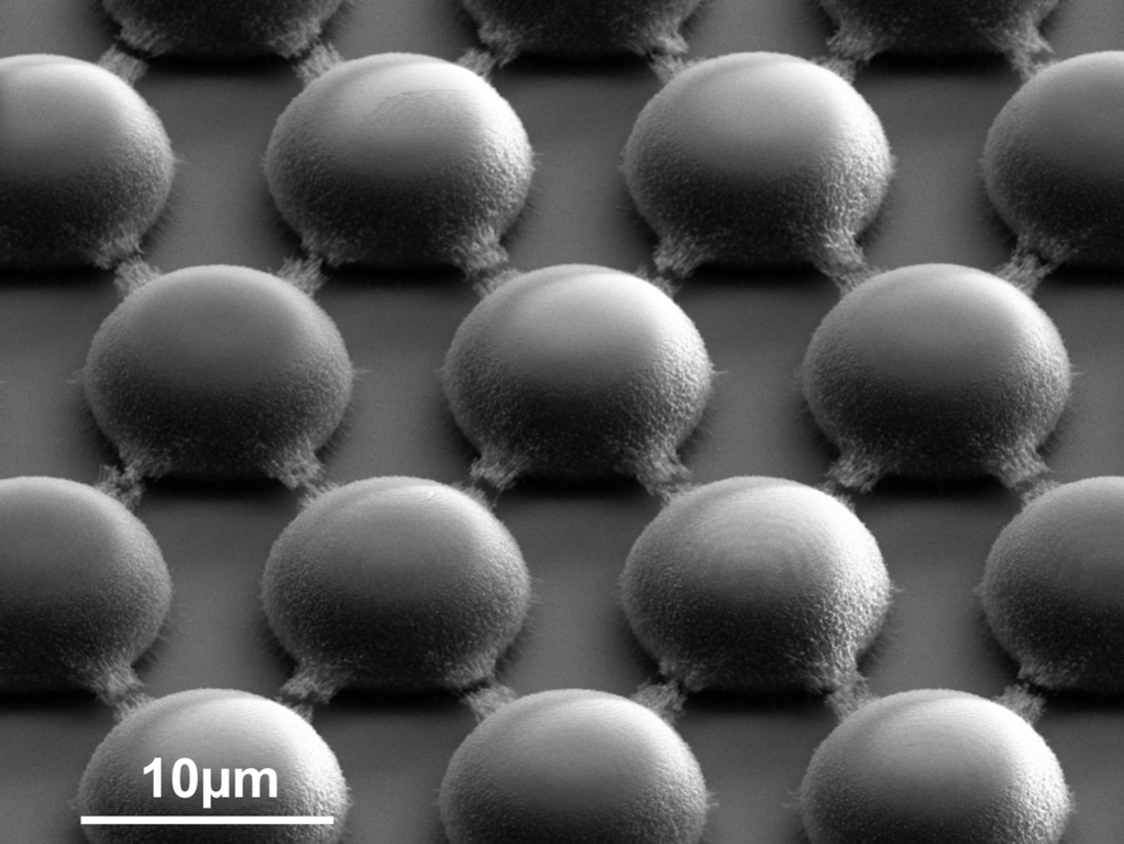
Title: “Micro Mine Field”
Description:
Micro-spheres of 7.5µm thick SU-8 resist exposed by EBL with 25kV.
Cross-linked resist exceeds the boundaries of the spheres and tries to reach the neighbor sphere.
This results in free standing bridges with gaps in between.
Magnification (3″x4″ image): 1.3KX
Instrument: RAITH150-TWO
Submitted by: Guido Piaszenski
Affiliation: Raith GmbH, Dortmund, Germany
Honorable Mention
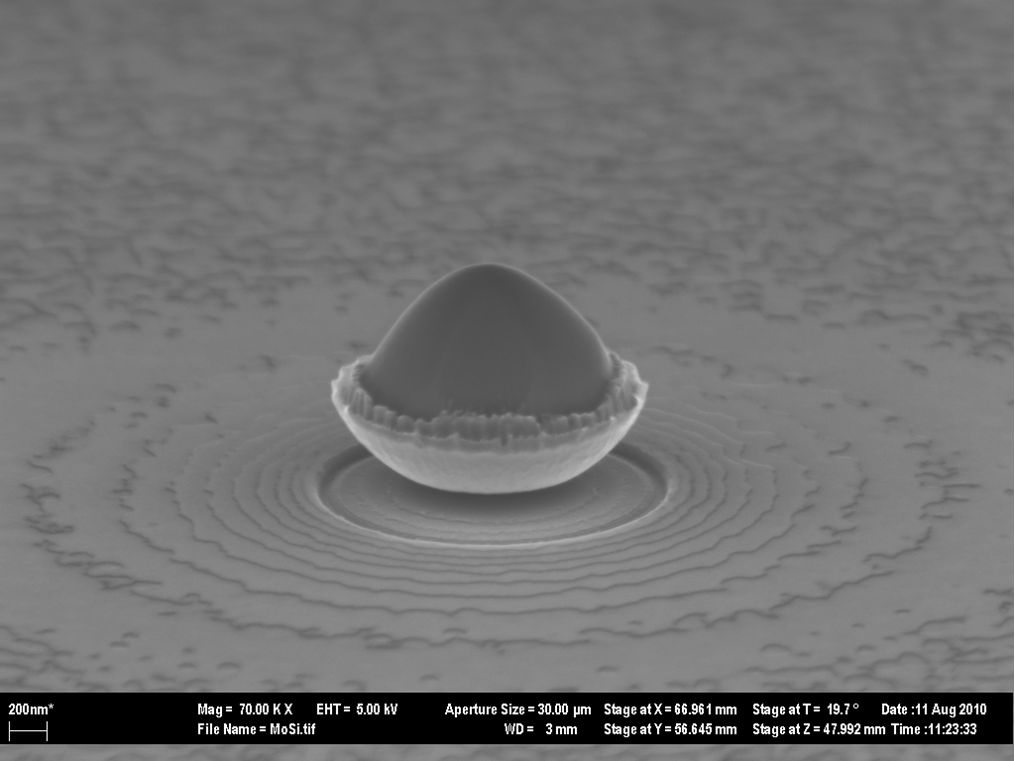
Title: “The nut in the Ice Age goes nano”
Description:
The nano nut of squirrel Scrap from Ice Age movie was found after etching Mo/Si multilayer with ICP.
Magnification (3″x4″ image): 70 KX
Instrument: Carl Zeiss, Supra 55VP
Submitted by: Birgit Päivänranta
Affiliation: Paul Scherrer Institut Villigen, Switzerland
Honorable Mention
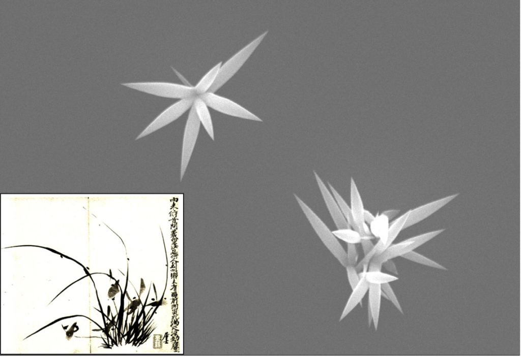
Title: “The Oriental Orchid”
Description:
The zinc oxide fibers look like the oriental orchid. The smooth curve of ZnO orchid shows beauty of orient
Magnification (3″x4″ image): 10KX
Instrument: JEOL, JSM-6500 P
Submitted by: Sang Han Park
Affiliation: Yonsei Univ. Seoul. Korea
Honorable Mention
Title: “Venice carnival mask” “Maschere di carnevale di Venezia”
Description:
– Pattern obtain by 2-photon polymerization of Poly-Ethylene-Glycol (PEG). – Overexposition of a 1µm line 2µm pitch lattice.
Magnification (3″x4″ image): 3.6KX
Instrument: Zeiss Ultra PLus
Submitted by: Thibault Honegger
Affiliation: BioColloNa – LTM-CNRS – UJF – CEA – Minatec
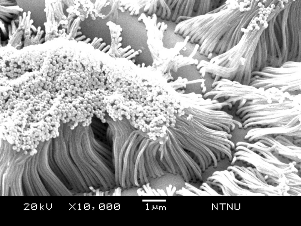
Honorable Mention
Title: “World Clocks”
Description:
Topview of deep holes etched in silicon. On the bottom of each hole resides a fishbone structure created during DRIE. In the final device, structures are supposed to stand upstraight in the middle of each hole, but in this case, the anisotropic etch profile has bent the fishbone structure at the bottom end, creating this dead fish farm.
Magnification (3″x4″ image): 13.9KX
Instrument: RAITH150
Submitted by: Sebastian Gautsch
Affiliation: Sensors Actuators and Microsystems Laboratory, EPFL, Neuchâtel, Switzerland
Honorable Mention
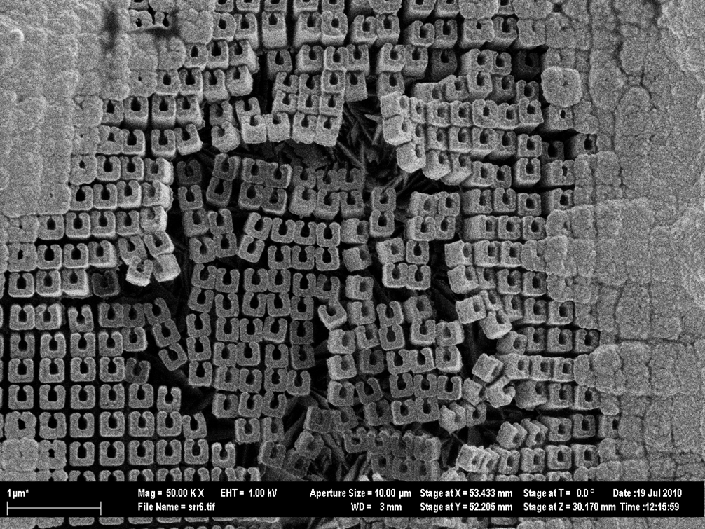
Title: “MNE 2011 Breaks Berlin Wall”
Description:
After electroplating of gold a small adhesion problem seemed to occur and all split rings looked like after an earthquake.
Magnification (3″x4″ image): 50KX
Instrument: Carl Zeiss, Supra 55VP
Submitted by: Birgit Päivänranta
Affiliation: Paul Scherrer Institut Villigen, Switzerland
Honorable Mention
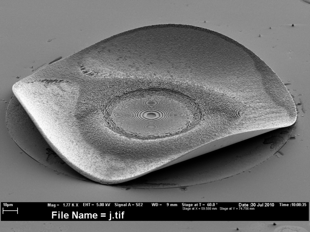
Title: “Throw Away Your Old Vinyl LPs”
Description:
Stress in an overplated Fresnel zone plate made of Au caused it to bow and delaminate from the substrate.
Magnification (3″x4″ image): 1.77KX
Instrument: Carl Zeiss, Supra 55V
Submitted by:Sergey Gorelick
Affiliation: Paul Scherrer Institut Villigen, Switzerland
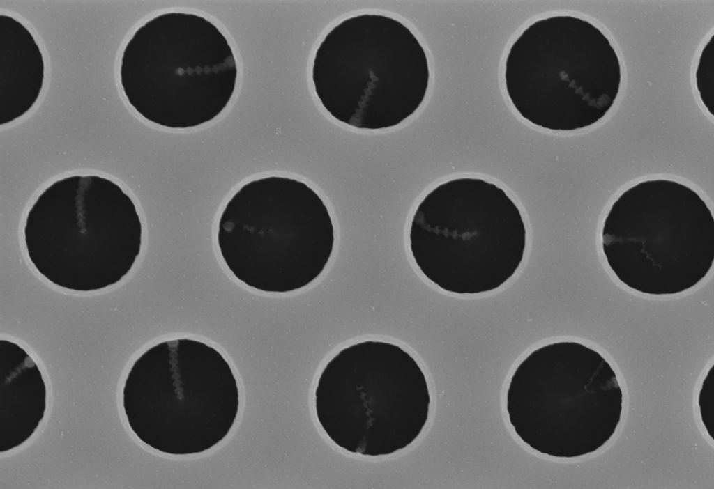
Honorable Mention
Title: “Jelly Fish”
Description:
Defective HSQ grating after e-beam lithography and development.
Can you find a mosquito and a moth?
Magnification (3″x4″ image): 25KX
Instrument: SEM Zeiss Supra 55VP
Submitted by: Vitaliy A,Guzenko
Affiliation: Paul Scherrer Institut
Honorable Mention
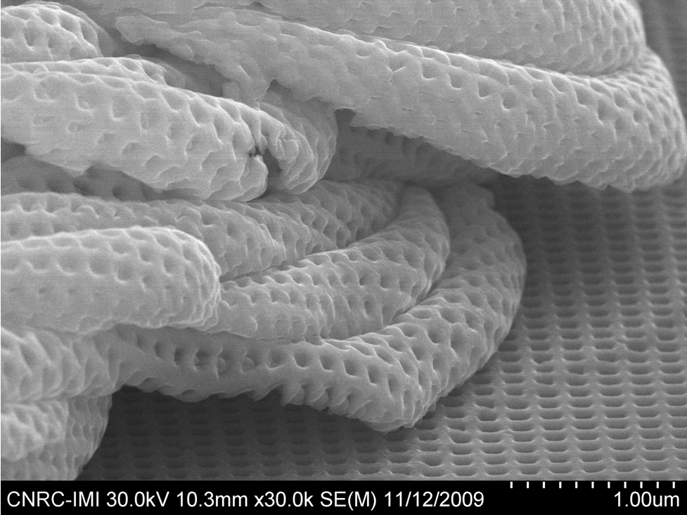
Title: “Put your nano towels on the floor to change”
Description:
Wrinkling in a patterned gold film
Magnification (3″x4″ image): 30KX
Instrument: Hitachi 4800
Submitted by: Keith Morton
Affiliation: National Research Council Canada
Honorable Mention
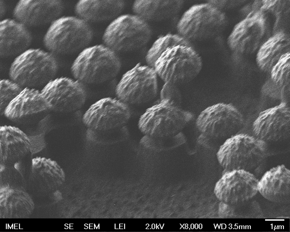
Title: “Dr Livingston has not visited this village yet”
Description:
Ps etched Particles on polymer substrate.
Magnification (3″x4″ image): 8KX
Instrument: Jeol-Jsm-7401F-Feg Sem
Submitted by: Ellinas Kosmas
Affiliation: NSCR Demokritos, IMEL Athens, Greece
Honorable Mention
Title: “Save the Forest ”
Description:
The silicon nanowires (SiNW) was formed by nanobead lithography and catalytic etching, the too long SiNW became curved.
Magnification (3″x4″ image): 10KX
Instrument: JEOL JSM – 6360
Submitted by: Mao-Jung Huang and Chii-Rong yang
Affiliation: ITRC, NARL, Taiwan National Taiwan normal university, Taiwan