1996→ |
The 39th International Conference on Electron,
Ion and Photon Beam Technology and Nanofabrication Bizarre/Beautiful Micrograph Contest
“A good Micrograph is worth more than the MegaByte it consumes.”
Results Submitted by John Randall
1995 Electron, Ion and Photon Beam Technology and Nanofabrication
Conference Chairman.
- Best Electron Micrograph
- Best Ion Micrograph
- Best Photon Micrograph
- Best Scanning Probe Micrograph
- Most Bizarre
- Grand Prize
The rules included the following:
- Contestants must be registered 1995 conference attendees.
- Micrographs must be sumbitted in slide format.
- Entries must be a single image taken with a microscope and may not be significantly altered.
- There is no restriction with respect to the subject matter.
- Electron and ion micrographs must be black and white.
Over 70 entries were submitted with the largest number being electron micrographs. There were many outsanding micrographs. Three of the winners demonstrate evidence of “what went wrong”. This is entirely appropriate for research at the frontiers of nanofabriaction. The panel of judges who selected the award winners consisted of:
Harold Craighead
Director of the National Nanofabrication Facility at Cornell University.
Evelyn Hu
Director of Quest, University of California at Santa Barbara.
Yasuo Iida
Research and Operational Planning Manager, Microelectronics Research Laboratories, NEC Corporation
Visitor count: accesses since June, 1997.
1996 Micrograph Contest Winners
1997 Micrograph Contest Winners
EIPBN Micrograph Contest Rules
Back to EIPBN Home Page
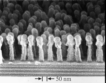
Best Electron Micrograph
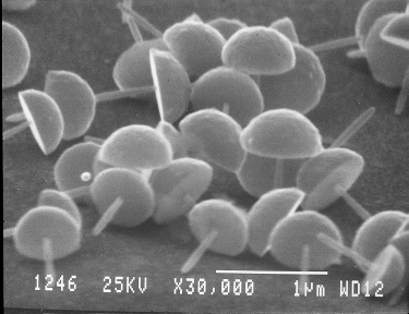
Title: Nano Thumbtacks
Magnification: 30,000X
Instrument: JEOL 840A Scanning Electron Microscope
Submitted by: Peter Krauss and Stephen Chou, Nanostructure Laboratory, University of Minnesota
Best Ion Micrograph
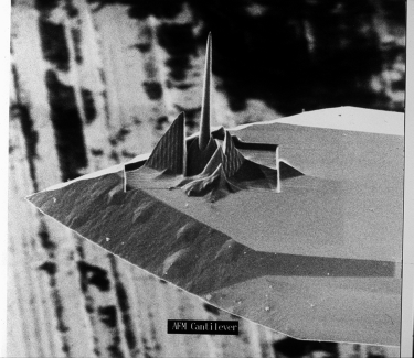
Title: “Focused ion beam (FIB) image of FIB micromachined AFM stylus”
Magnification: 5,000X
Instrument: Micrion model 9100 FIB system
Submitted by: Bill Thompson and Randy Lee, Micrion Corporation
Best Optical Micrograph
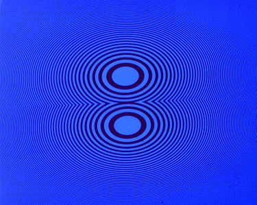
Title:”Two Stones on the Water”
Magnification: 12X
Instrument: Optical Microscope Technival (Jenoptik, Germany)
Submitted by: Sergey Babin, Physics and Technology Institute, the Russian Academy of Sciences
Best Scanning Probe Micrograph
Title: “The Lost Picasso”
Magnification: 250,000X
Instrument: East Coast Scientific STM insitu in VG MBE System
Submitted by: Stuart Brown, Mike Grimshaw, Geb Jones, University of Cambridge U.K.
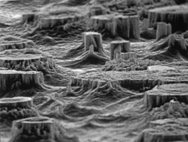
Most Bizarre Micrograph
Title: The Debutantes’ Ball
Description: The micrograph shows an array of 50nm-wide posts with a periodicity of 100nm. The posts consist of PMMA on top of an Anti-Reflection Coating (ARC). The substrate consists of a 250nm-thick layer of silicon nitride on silicon. The PMMA was exposed using Achromatic Interferometric Lithography. After development of the PMMA, an O2 Reactive Ion Etch was used to etch through the ARC. SEM viewing caused some melting and charging which resulted in the large gathering of nano-women. The melting problem was solved by imaging at low voltage.
Magnification: 100,000X
Instrument: Zeiss DSM982 Gemini Scanning Electron Microscope
Submitted by: Tim Savas, Massachusetts Institute of Technology
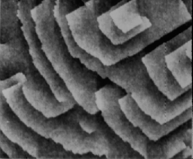
Grand Prize Micrograph
Title: GaAs Grand Canyon
Magnification: 10,000X
Instrument: Cambridge S360 Scanning Electron Microscope
Submitted by: Chris Youtsey, University of Illinois
1996 Micrograph Contest Winners
Back to Home EIPBN MicroGraph Contest
Back to EIPBN Home Page