Atomically precise manufacturing — building
at the molecular scale with engineering control — is the
ultimate Grand Challenge of the National Nanotechnology Initiative.
Only a few years ago, this goal sounded like science fiction, but
recent scientific results show it is within our grasp, if we rise
to the challenge. Developing and commercializing this technology
will deliver substantial economic, social, defense, and health
benefits to our country—and society in general. Some frequently
asked questions and answers concerning this revolutionary technology
follow.
Atomically precise manufacturing is the ability
to manufacture materials and structures at the atomic or molecular
size scale. This technology integrates the knowledge and low
manufacturing cost of chemistry with the knowledge and flexibility
of engineering. The result is a manufacturing technology that
achieves the low cost of chemical manufacturing, combined with
the engineering mastery that brings us the microchip or suspension
bridges, and the flexibility and design freedom offered by computer
software. This future manufacturing technology will enable us
to make products in a cleaner, cheaper, and faster way than any
technology that exists today.
Self-assembly is a powerful process for creating
materials, and a number of research groups are experimenting in the
field. Zyvex will utilize some aspects of self-assembly, but the
core focus of our technical approach is to create engineered structures
by means of parallel, automated assembly of atoms under computer
control. This positionally-controlled chemistry allows us to achieve
the long-range order of molecular-scale building blocks that is vital
to atomically precise manufacturing. On the other hand, self-assembly
is sensitive to slight changes in the building blocks, making those
systems difficult to engineer. It also suffers from a lack of long-range
order. As an example, imagine building a 200-foot brick wall. A pure
self-assembly approach would start by randomly laying twenty bricks
and building up from each brick independently. One would soon find
that the random sections didn’t join with one another, and
the resulting brick wall would be weak and ugly. Zyvex’s ordered
approach to assembly would start by laying a foundation row of bricks,
and building up from there row by row. Long-range order is extremely
important to engineering strong, useful structures.
Actually we agree with Professor Smalley. However,
if you look carefully at what he has said, it does not apply to
our approach. Smalley believed that complex, floppy molecules cannot
be put together with atomic pick and place techniques. Our target
is not the kinds of molecules that living creatures make, but rather
rigid, crystalline structures comprised of a small number of elements.
Our approach will use parallel arrays of molecular-scale tools
operating with high precision to create extremely valuable devices
and structures with atomic precision.
Some implications of quantum mechanics are hard
to understand, which leads to certain myths about quantum uncertainty.
The uncertainty of any particle’s position is related to its
momentum (or mass), so while a light electron may have considerable
uncertainty in its position and momentum, an atom is much heavier
and tends to stay put (which also keeps its electrons nearby). If
atoms were as frisky as the “quantum uncertainty” critics
claim, solid objects would continually evaporate before our eyes
(in fact, life could not exist in such a universe).
|
Figure
1.
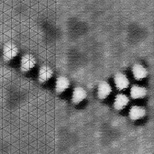
IBM’s molecular cascade 3-input sorter. CO molecules are arranged
on Cu to perform a logic function.
Figure 2.
Oxygen atoms arranged on Pt surface from “Single Molecule Dissociation
by Tunneling Electrons,” B.C. Stipe, M.A. Rezaei, W. Ho, S. Gao,
M. Mersson, and B.I. Lundqvist. Phys. Rev. Lett. 78 (1997): 4410-4413.
Figure
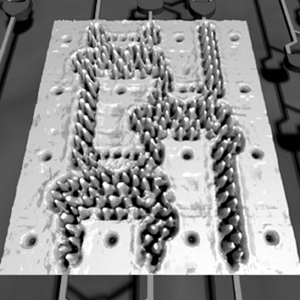
3.
Assembled Iron and Cu Carbonyls by Wilson Ho from “Structural Determination
by Single-Molecule Vibrational Spectroscopy and Microscopy: Contrast
Between Copper and Iron Carbonyls.” H.J. Lee and W. Ho, Phys. Rev.
B. 61 (2000): R16347-R16350.
Figure
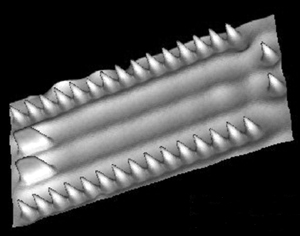
4.
Molecular accelerator created on Cu surface by Saw Hla, Ohio University.
|
Yes. The first clear demonstration of the arrangement of atoms was in
1990 when Don Eigler arranged 35 Xenon atoms to spell out IBM.1 Since
then, many groups have demonstrated the ability to manipulate atoms into
designed structures. Bob Celotta and Joe Stroscio of the National Institute
of Standards and Technology (NIST) have gone so far as to make the Autonomous
Atom Assembler that can create designed arrangements of atoms in a completely
automated fashion.2 Eigler’s team has
recently created molecular logic structures (see Figure 1 at left).
As a matter of fact, yes. Wilson Ho3 at UC
Irvine, and Saw Hla4 at Ohio University have
manipulated atoms and molecules to make and break chemical bonds (see
Figures 2 thru 4). Figure 3 shows a clear demonstration of what we call
mechanochemistry — where we can move atoms and molecules together
to deliberately make and break chemical bonds.
Yes, it has. Joe Lyding5 at the University
of Illinois Urbana-Champaign has shown that he can remove hydrogen atoms
adsorbed on atomically flat silicon surfaces. We refer to this as “atomic
precision depassivation.” Michelle Simmons6 at
the University of New South Wales has used this technique to place a
single phosphorous atom at an exact location in a silicon lattice to
form a “Qubit” (the fundamental computing element in quantum
computation). Lyding7 has recently shown
that he can control the growth of single layers of atoms with his depassivation
technique to make three-dimensional structures of crystalline silicon.
It is well known that atoms are in a state of constant motion due to
thermal noise. In liquids, small particles are jostled around by the
liquid molecules; an effect called “Brownian motion.” The “thermal
noise” critics claim it isn’t possible to build with atomic
precision due to this effect. However, careful analysis shows that stiff
structures can hold their position with high accuracy even in the presence
of thermal noise. This is proven by thousands of researchers worldwide
making atomic resolution pictures of atomic structures, and doing the
atomically precise manipulations described earlier. If we choose to make
our positioning devices with less stiffness, we can cool the environment,
which reduces thermal vibration to inconsequential levels. This is not
a problem that will stop our progress.
The most valuable structures that could be made with this technique would
be tools to enable modestly parallel initially, and then massively parallel
systems to produce atomically precise structures more cost effectively.
But there are many highly valuable very small structures that could be
made with a tool that could only assemble things one atom at a time.
One entire class of structures is designed to interact with specific
molecules. One example of this is a nanopore that would have the ability
to read DNA at up to one million bases per second.8,9 Atomically
precise tips for atomic force and scanning tunneling microscopes would
have a huge impact on metrology for the semiconductor industry and for
science in general. Earlier in this white paper, we mentioned qubit for
quantum computing.6 It takes just a handful
of qubits to do quantum encryption. There are many other highly valuable
products that one could create with early stage atomically precise manufacturing
tools.
|
Science fiction writers love to use a little pseudo-science to tell a good
story, but we shouldn’t confuse pseudo-science with reality. We intend
to build machines that help us manufacture things with atomic precision. This
is grounded in reality, as evidenced in the research we mentioned earlier.
Building self-aware machines that reproduce in the wild is science fiction,
and likely to remain that way for many decades, even at the macro scale. Nobody
knows how to do this sort of thing even with supercomputers, computerized machine
shops, and unlimited electric power, so worrying about doing it in specks too
small to see, powered by fuel cells we don’t even know how to make, reproducing
themselves by some unknown technology, and programmed by genius programmers
that haven’t even built a robot as smart as a worm, seems a waste of
worry.
1. D.
M. Eigler, E.K. Schweizer. Nature 334 (1990): 524.
2. Celotta and Stroscio, “AVS Symposium.” Nov
2003.
3. See twelve papers by Wilson Ho on controlling
chemistry at the atomic scale.
4. See eleven papers by Saw Hla on his work on chemistry
at the atomic scale.
5. See eight papers by Joe Lyding of hydrogen depassivation.
6. See ten papers by Michelle Simmons on constructions
of qubits.
7. Joe Lyding described Patterned ALE at the “AVS
Symposium.” March 2003.
8. Dan Branton, Harvard. http://www. mcb.harvard.edu/brantonindex.htm.
9. Viktor Stolc. “Nanopores for Gene Sequencing.” Proposal.
NASA Ames Research Center.
• L.J. Lauhon and
W. Ho, “The Initiation and Characterization of Single Bimolecular
Reactions with a STM.” Faraday Discussion 117 (2000): 249-255.
• L.J. Lauhon and W. Ho. “Inducing and Observing the Abstraction
of a Single Hydrogen Atom in Bimolecular Reaction with a Scanning Tunneling Microscope.” J.
Phys. Chem. 105 (2000): 3987-3992.
• G. V. Nazin, X. H. Qiu, and W. Ho. “Visualization and Spectroscopy
of a Metal-Molecule-Metal Bridge.” Science 302 (2003): 77-81. Published
online September 4, 2003; 10. 1126/Science. 1088971.
• T. M. Wallis, N. Nilius, and W. Ho. “Single Molecule Vibrational
and Electronic Analyses of the Formation of Inorganic Complexes: CO Bonding to
Au and Ag Atoms on NiAl [110].”
J. Phys. Chem. 119 (2003): 2296-2300.
• N. Nilius, T. M. Wallis, and W. Ho. “Vibrational Spectroscopy and
Imaging of Single Molecules: Bonding of CO to Single Palladium Atoms on NiAl[110].” J.
Phys. Chem. 117 (2002): 10947-10952.
• W. Ho. “Single Molecule Chemistry.” J. Phys. Chem. 117 (2002):
11033-11061.
• T. M. Wallis, N. Nilius, and W. Ho. “Electronic Density Oscillations
in Gold Atomic Chains Assembled Atom by Atom.” Phys. Rev. Lett., 89 (2002):
236802.
• J.R. Hahn and W. Ho. “Oxidation of a Single Carbon Monoxide Molecule
Manipulated and Induced with a Scanning Tunneling Microscope.” Phys. Rev.
Lett. 87 (2001): 166102.
• L.J. Lauhon and W. Ho. “Single Molecule Chemistry and Vibrational
Spectroscopy: Pyridine and Benzene on Cu [001].” J. Phys. Chem. A, 104
(2000): 2463-2467.
• L.J. Lauhon and W. Ho. “Control and Characterization of a Multi-step
Unimolecular Reaction.” Phys. Rev. Lett. 84 (2000): 1527-1530.
• H.J. Lee and W. Ho. “Single Bond Formation and Characterization
with a Scanning Tunneling Microscope.” Science, 286 (1999): 1719-1722.
• B.C. Stipe, M.A. Rezaei, W. Ho, S. Gao, M. Persson, and B.I. Lundqvist. “Single
Molecule Dissociation by Tunneling Electrons.” Phys. Rev. Lett., 78, 4410.
• S.W. Hla, K.F.
Braun, K.H. Rieder. Phys. Rev. B, 67 (2003): 201402(R).
• S.W. Hla, K.H. Rieder. Ann. Rev. Phys. Chem. 54 (2003): 307-330.
• S.W. Hla, G. Meyer, K.H. Rieder. Chem. Phys. Lett. 370 (2003): 431-436.
• S.W. Hla. “Nanoscale spectroscopy and its application in semiconductor
research.” Edited by Y. Watanabe, S. Heun, G. Salviati, N. Yamamoto. Lecture
Notes in Physics (Springer Verlag Heidelberg), (2002): 222-230.
• S.W. Hla, K.H. Rieder. “Superlattices & Microstructures.” 31
(2002): 63-72.
• A. Kühnle, G. Meyer, S.W. Hla, K.H. Rieder. Surf. Sci. 499 (2002):
15-23.
• G. Meyer, F. Moresco, S.-W. Hla, J. Repp, K.-F. Braun, S. Foelsch, K.H.
Rieder. Jap. J. Appl. Phys. 40 (2001): 4409-4412.
• S.W. Hla, G. Meyer, K.H. Rieder. “Inducing Single Molecule Chemical
Reactions with STM: A New Dimension for Nano-Science and Technology.” Chem
Phys Chem. 2 (2001): 361-366.
• S.W. Hla, L. Bartels, G. Meyer, K.H. Rieder. “Inducing all steps
of a chemical reaction with the scanning tunneling microscope tip: Towards single
molecule engineering.” Phys. Rev. Lett. 85 (2000): 2777-2780.
• S.W. Hla, A. Kuhnle, G. Meyer, K.H. Rieder. “Controlled lateral
manipulation of single diiodo-benzene molecules on the Cu surface with the tip
of a scanning tunneling microscope.” Surf. Sci. 454-456 (2000): 1079.G.
Meyer, J. Repp, S. Zöphel, K.F. Braun, S.W. Hla, S. Fölsch, L. Bartels,
F. Moresco, K.H. Rieder. “Controlled manipulation of atoms and small molecules
with a low temperature scanning tunneling microscope.” Single Molecule
1 (2000): 79-86.
• M. C. Hersam,
N. P. Guisinger, and J.W. Lyding. “Silicon-based molecular
nanotechnology.” Nanotechnology 11 (2000): 70.
• G.C. Abeln, M.C. Hersam, D.S. Thompson, S.T. Hwang, H. Choi, J.S. Moore,
and J.W. Lyding. “Approaches to Nanofabrication on Si Surfaces: Selective
Area CVD of Metals and Selective Chemisorption of Organic Molecules.” J.
Vac. Sci. Technol. B 16 (1998): 3874.
• M. C. Hersam, J. Lee, N. P. Guisinger, and J.W. Lyding. “Implications
of atomic-level manipulation on the Si [100] surface: From enhanced CMOS reliability
to molecular nanoelectronics.” Superlattices and Microstructures 27 (2000):
583.
• M.C. Hersam, G.C. Abeln, and J.W. Lyding, “An Approach for Efficiently
Locating and Electrically Contacting Nanostructures Fabricated via UHV-STM Lithography
on Si [100].” Micro-electronic Engineering 47 (1999): 235.
• I.C. Kizilyalli, K. Hess, and J.W. Lyding, “Channel Hot Electron
Degradation-delay in MOS Transistors Due to Deuterium Anneal.” The VLSI
Handbook Chapter 13. CRC Press LLC. (1999).
• J. Lee, Y. Epstein, A.C.erti, J. Huber., K. Hess, and J.W. Lyding. “The
Effect of Deuterium Passivation at Different Steps of CMOS Processing on Lifetime
Improvements of CMOS Transistors,” IEEE Transactions on Electron Devices,
46 (1999): 1812.
• J.W. Lyding, K. Hess, G.C. Abeln, G.C. Thompson, J.S. Moore, M.C. Hersam,
E.T. Foley, J. Lee, Z. Chen, S.T. Hwang, H. Choi, P.H. Avouris, and I.C. Kizilyalli, “UHV-STM
Nano-fabrication and Hydrogen/Deuterium Desorption from Silicon Surfaces: Implications
for CMOS Technology,” Applied Surface Science, 130-132 (1998): 221.
• Foley, E. T., Kam, A. F., Lyding, J. W., and Avouris, P. H. “Cryogenic
UHV-STM Study of Hydrogen and Deuterium Desorption from Si [100],” Physical
Review Letters, 80/6 (1998): 1336-1339.
• J.L. O’Brien,
S.R. Schofield, M.Y. Simmons, R.G. Clark, A.S. Dzurak, N.J. Curson,
B.E. Kane, N.S. McAlpine, M.E Hawley and G.W. Brown. “Towards
the fabrication of phosphorus qubits for a silicon quantum computer”,
Phys. Rev. B, 64 (2001): 161401.
• L. Oberbeck, N.J. Curson, M.Y. Simmons, R. Brenner, A.R. Hamilton, S.R.
Schofield and R.G. Clark. “Encapsulation of phosphorus dopants in silicon
for the fabrication of a quantum computer.” Applied Physics Letters 81
(2002): 3197.
• A.S. Dzurak, M.Y. Simmons, A.R. Hamilton, R.G. Clark, R. Brenner, T.M.
Buehler, N.J. Curson, E. Gauja, R.P. Mckinnon, L.D. Macks, M. Nitic, J.L. O’Brien,
L. Oberbeck, D.J. Reilly, S.R. Schofield, F.E. Stanley, D.N. Jamieson, S. Prawer,
C. Yang and G.J. Milburn/ “Construction of a silicon-based solid state
quantum computer.” Quantum Information and computation 1 (2001): 82.
• J.L. O’Brien, S.R. Schofield, M.Y. Simmons, R.G. Clark, A.S. Dzurak,
N.J. Curson, B.E. Kane, N.S. McAlpine, M.E. Hawley and G.W. Brown. “Nanoscale
phosphorus atom arrays created using STM for the fabrication of a silicon based
quantum computer.” BioMEMS and Smart Nanostructures 4590 (2001): 299.
• J.L. O’Brien, S.R. Schofield, M.Y. Simmons, R.G. Clark, A.S. Dzurak,
N.J. Curson, B.E. Kane, N.S. McAlpine, M.E. Hawley, and G.W. Brown. “Scanning
tunneling microscope fabrication of arrays of phosphorus atom qubits for a silicon
quantum computer.” Smart Materials and Structures 11 (2002): 741.
• M.E. Hawley, G.W. Brown, M.Y. Simmons and R.G. Clark. “Fabricating
a qubit array with a scanning tunneling microscope.” Los Alamos Science
27 (2002): 302.
• M. Y. Simmons, S. R. Schofield, J. L. O’Brien, N. J. Curson, L.
Oberbeck, T. Hallam and R. G. Clark. “The atomic-scale fabrication of a
solid-state silicon based quantum computer.” Surface Science. July 2002.
• N.J. Curson, S.R. Schofield, M.Y. Simmons, L. Oberbeck and R.G. Clark. “Critical
issues in the formation of atomic arrays of phosphorus in silicon for the fabrication
of a solid-state quantum computer.”Surface Science. July 2002.
• L. Oberbeck, N.J. Curson, M.Y. Simmons, S.R. Schofield and R.G. Clark, “Challenges
in surfaces for quantum computing.” Surface Review and Letters. August
2002.
• L. Oberbeck, T. Hallam, N.J. Curson, M.Y. Simmons and R.G. Clark, “Epitaxial
silicon growth in the presence of hydrogen.” Applied Surf. Sci. (2002).
© 2004-2010,
Zyvex Labs, LLC. |