←2011 |
2013→ |
MNE 2012 Micro Nano Graph Contest
“ A good Micrograph is worth more than the MegaByte it consumes.”Entries Presented by Dr. John Randall – Zyvex Labs Sponsored by
The rules include the following:
• Entries have to be of a single image taken with a microscope and not significantly altered.
• There is no restriction with respect to the subject matter.
• Electron and ion micrographs have to be black and white.
In 2012, 53 entries were submitted. There were many outstanding micrographs. The work represented in the submitted micrographs covered a wide range of fields including micro mechanical, photonic, and integrated circuit fabrication, chemical and dry etching, laser optics, carbon nanotube structures, biological samples, material science experiments and, of course, e-beam, ion beam, and nano imprint lithography experiments.
The panel of judges who selected the award winners were:
- Gerard BenAssayag – CEMES-CNRS
• Don & Judy Tennant – Cornell
• Rebecca Ballard – UT Dallas
The Awards are:
• First Prize
• Second Prize
• Third Prize
The judges also selected 7 Honorable Mentions.
All 2012 Entries (with original titles)
Judges exercised their prerogative to change the micrograph titles if it pleased them.
First Prize
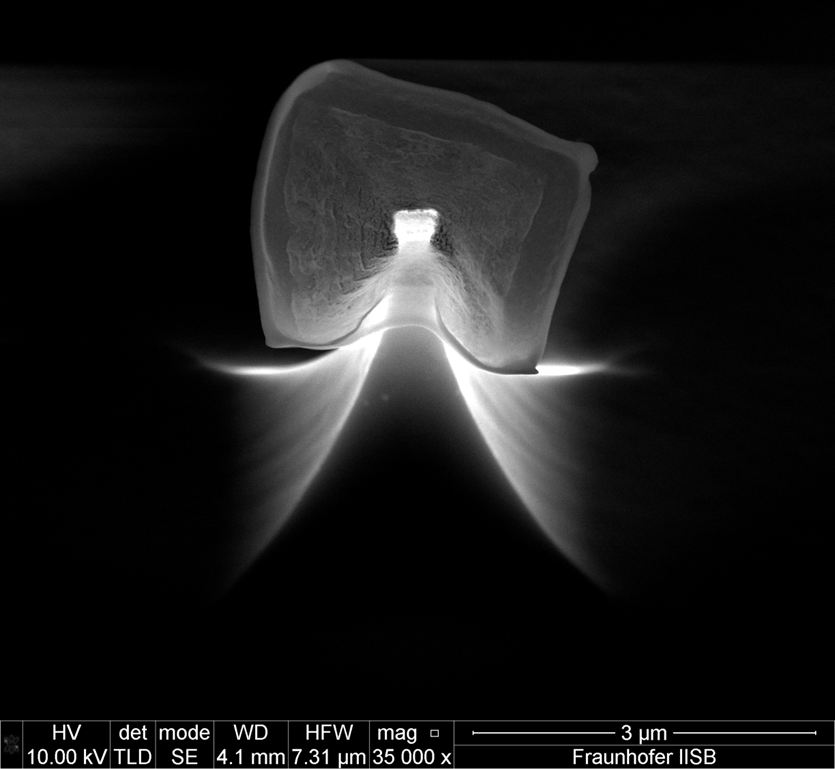
Title: La Princesse Angelique
Description:
Ga+ resistless lithography together with rather isotropic RIE. The etch mask still exists on top. Only if you go beyond the surface you will discover.
Magnification (3″x4″ image): 35kX
Instrument: FEI Helios Nanolab 600
Submitted by: Mathias Rommel, Maximilian Rumler
Affiliation: Fraunhofer IISB, Erlangen, Germany
Second Prize
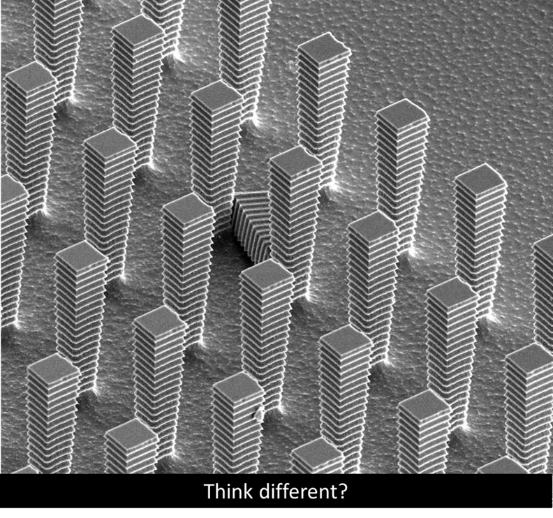
Title: One Down . . . ?
Description:
Silicon pillars etched by Bosch Process. 5x5x20um with pitch 9um. Intended to be super hydrophobic surface.
Magnification (3″x4″ image): 5KX
Instrument: FEI
Submitted by: Dr. Andrea Notargiacomo, Dr. Annamaria Gerrdino
Affiliation: CNR-IFN Institute for photonics and Nanotechnology, Rome, Italy
Third Prize
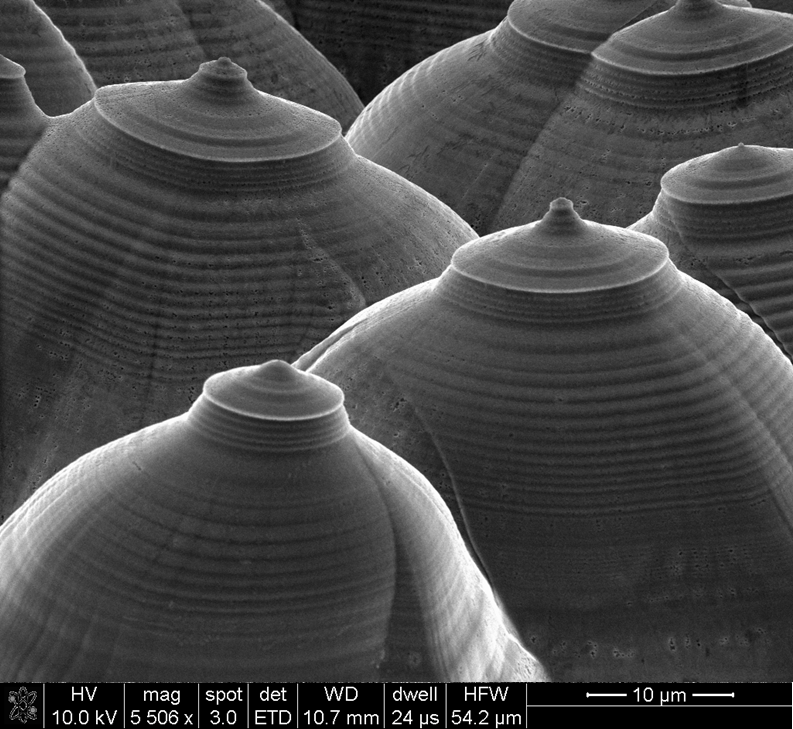
Title: Ceramic Jugs
Description:
Surface of electroplated Nickel shadow mask after SU-8 template removal in Piranha.
Magnification (3″x4″ image): 5.5KX
Instrument: FEI NOVA SEM 600
Submitted by: Stephan S. Keller
Affiliation: DTU Nanotech, Denmark
Honorable Mention
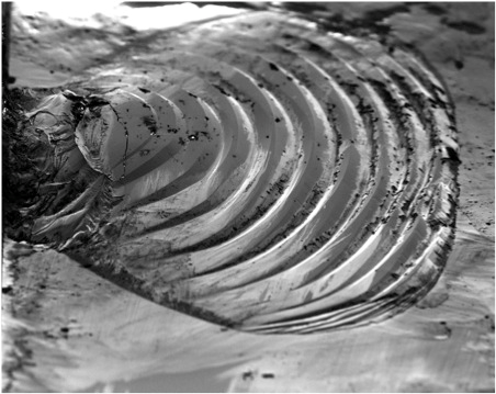
Title: Nano on the half shell
Description:
A stage for the smallest actors; the ruins, perhaps, of a once mighty(small) civilization. (Micrograph was originally entitled “Amphitheatre”.
Magnification (3″x4″ image): 450 X
Instrument: Zeiss Ultra55
Submitted by: Steven Hickman
Affiliation: Harvard Center for Nanoscale Systems, Cambridge, USA
Honorable Mention
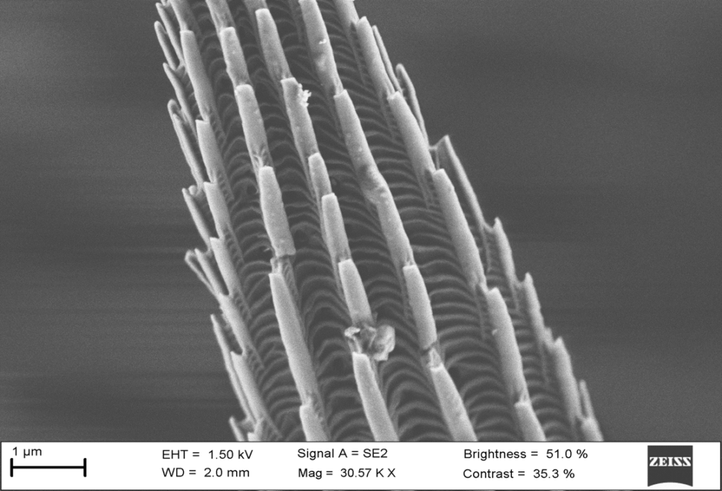
Title: Chicago Parking Structure
Description:
The bright tower appears in grey-scale at SEM, but it shines with wonderful shimmering colours in sunlight.
Magnification (3″x4″ image): 30.57 KX
Instrument: Zeiss FESEM Ultra Plus
Submitted by: Manuel Gomez
Affiliation: CIQUS, Center for Research in Biological Chemistry and Molecular Materials, Santiago de Compostela University, Galicia, Spain
Honorable Mention
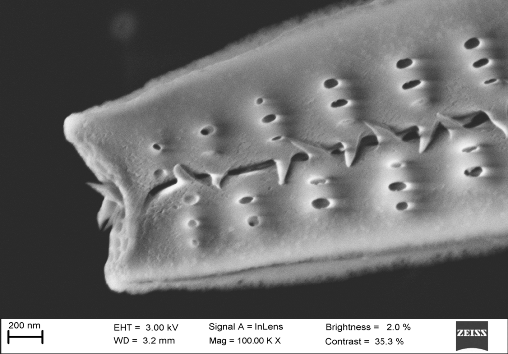
Title: Alligator Gingivitis
Description:
Deep in the darkness of the nanoworld live some dangerous monsters with hundreds of sharp teeth and eyes. As Tweety says: I thought I taw an itty, bitty puddy tat
Magnification (3″x4″ image): 100KX
Instrument: Zeiss FESEM Ultra Plus
Submitted by: Manuel Gomez
Affiliation: CIQUS, Center for Research in Biological Chemistry and Molecular Materials, Santiago de Compostela University, Galicia, Spain
Honorable Mention
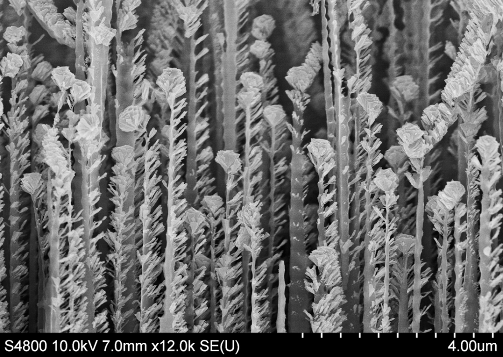
Title: Fleur de Femto
Description:
Our contribution to “Green” manufacturing! These roses thrive and prosper only unter extreme conditions: vacuum, climate-wrecking gases, no sunshine and without water! You have no idea how long it took me to grow these little roses only with the capabilities of an ICP Plasma reactor!
Magnification (3″x4″ image): 12KX
Instrument: Hitachi S4800
Submitted by: Martin Hoffmann
Affiliation: Ilmenau University of Technology, Ilmenau, Germany
Honorable Mention
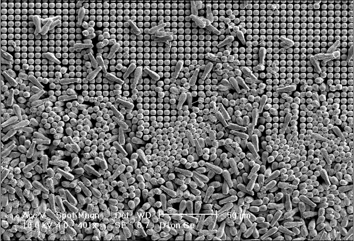
Title: Order vs Chaos
Description:
Breaking of GaAs pillars grown on pre-patterned silicon substrate. The disorder has been caused by an incorrect cleaving step.
Magnification (3″x4″ image): 401X
Instrument: Philips XL30 SFEG SEM
Submitted by: Monica Bollani
Affiliation: IFN_CNR, L-NESS laboratory, Como, Italy
Honorable Mention
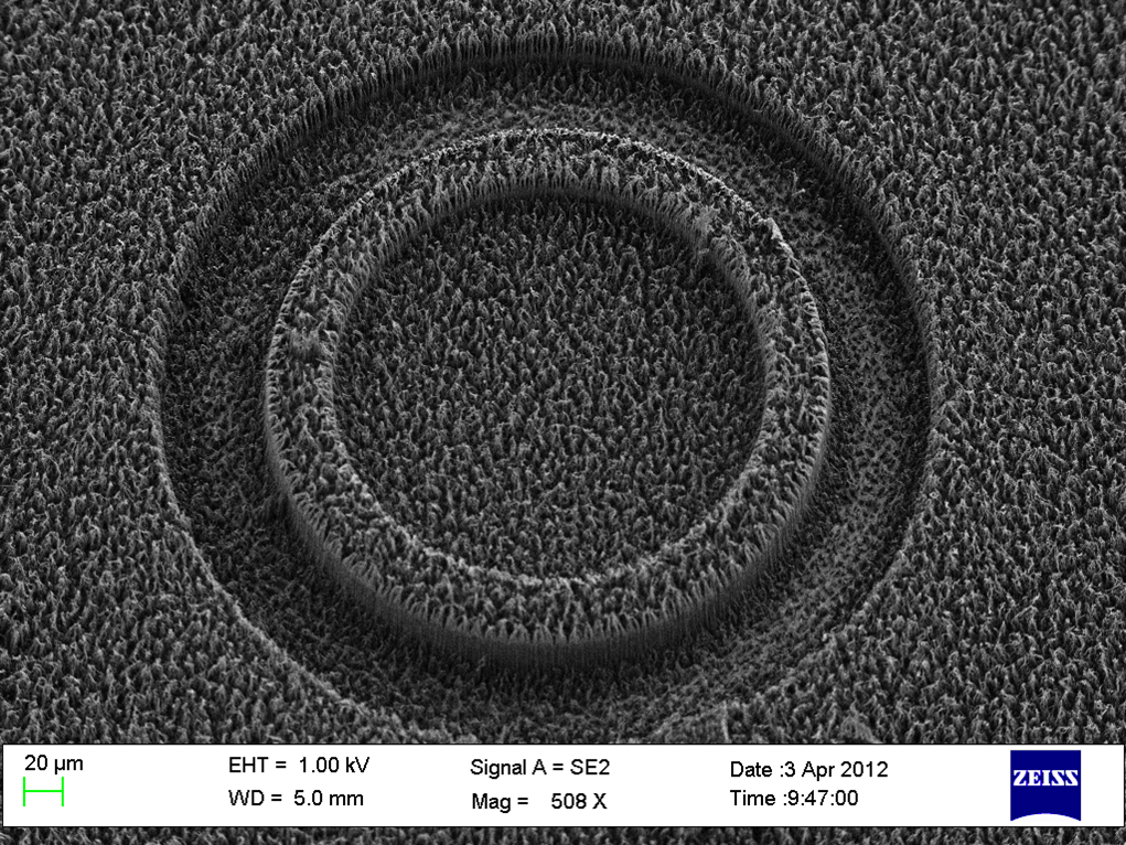
Title: Faerie Circle
Description:
Biodegradable polymer grass, crop circle
Magnification (3″x4″ image): 508X
Instrument: Zeiss, SEM
Submitted by:Johan Nagstrup
Affiliation: DTU nanotech, Technical University of Denmark, Denmark
Honorable Mention
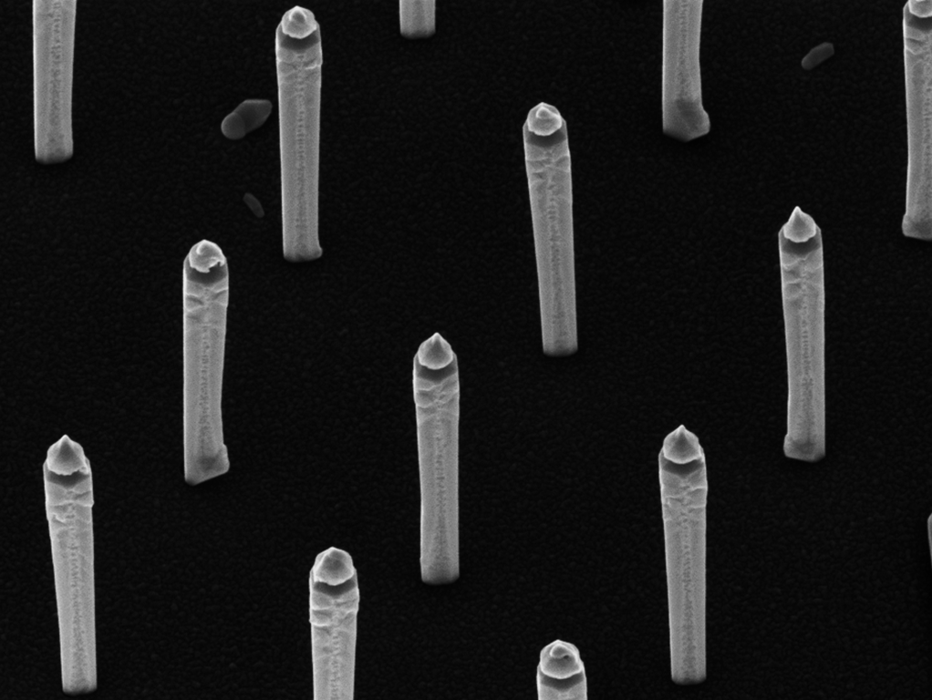
Title: Stiff in parallel
Description:
The SEM image illustrates an array of lithographically positioned single crystalline GaAs1-xSbx/Al1-xGaxAs core-shell semiconductor nanowire heterostructures, grown gold-free on Si(111) by molecular beam epitaxy. The shape of the “flame” is due to progressive crystallization of the Ga-rich droplet during the Al1-xGaxAs shell growth.
These elegant nanocandles are the first example of an antimonide nanowire array directly integrated on silicon, which promises the emergence of a whole family of novel infra-red and energy nanodevices.
Magnification (3″x4″ image): 20.67 KX
Instrument: Carl Zeiss, Supra 55VP
Submitted by:Dr. Xiang-Lei Han, Dr. Philippe Caroff
Affiliation: IEMN-CNRS UMR 8520, Villeneuve d’Ascq, France