←1996 |
1998→ |
Ion and Photon Beam Technology and Nanofabrication
Bizarre/Beautiful Micrograph Contest
“A good Micrograph is worth more than the MegaByte it consumes.”
Results Submitted by John Randall
- Best Electron Micrograph
- Best Ion Micrograph
- Best Photon Micrograph
- Best Scanning Probe Micrograph
- Most Bizarre
- Grand Prize
In addition the judges selected a number of micrographs for Honorable Mention Awards.
The rules included the following:
- Contestants must have been registered 1997 conference attendees.
- Micrographs must be submitted as an 8 inch by 10 inch and must be accompanied by a completed entry sheet.
- Entries must be of a single image taken with a microscope and may not be significantly altered.
- There is no restriction with respect to the subject matter.
- Electron and ion micrographs must be black and white.
Over 40 entries were submitted. There were many outstanding micrographs. The work represented in the submitted micrographs covered a wide range of fields including micro mechanical, photonic, and integrated circuit fabrication, chemical and dry etching, field emission tips, UV and x-ray optics, and of course e-beam, ion beam, x-ray, and photo lithography experiments. While the largest number of entries were electron micrographs, the Most Bizarre prize winner was an optical micrograph. The panel of judges who selected the award winners consisted of:
Prof. Kenji Gamo
Director Gamo Lab, Osaka University
Evelyn Hu
Director of Quest, University of California at Santa Barbara.
Alexander Tritchkov
Optics Cluster, Litho Group IMEC, Belgium
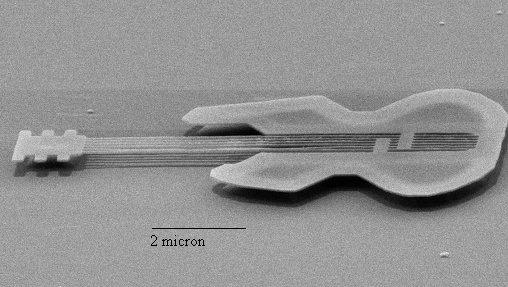
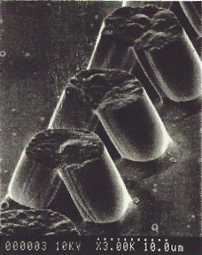
Title: World’s Smallest Non-Functional Guitar
Magnification: 16,500X
Instrument: Zeiss Leo DSM 982 Scanning Electron Microscope
Submitted by: Dustin Carr, Cornell University.
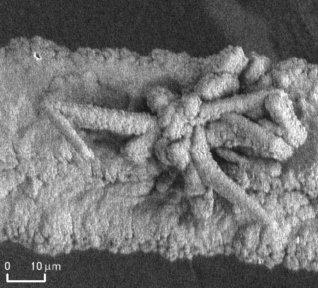
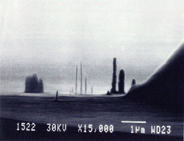
Title: There’s Still Life in GaAs
Magnification (for 4″ Height): 1250X
Instrument: Homebuilt in-situ ion beam/ MBE system.
Submitted by: G.A.C. Jones, and P.D. Rose, Cambridge University
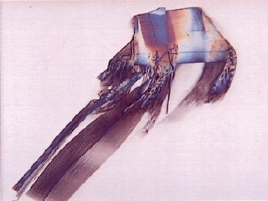
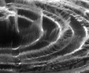
Title: Beware of the jelly fish!
Magnification (for 4″ image height): 400X
Instrument: Leitz Ergolux
Submitted by: Dr. F.C.M.J.M. van Delft and Dr.Ir. M.J. Verheijen, Philips Research, Eindhoven, The Netherlands
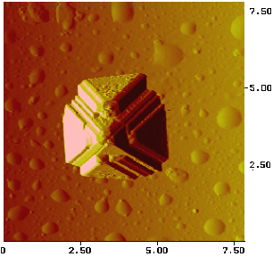
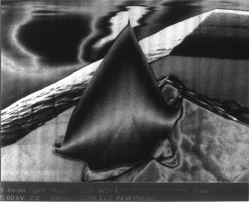
Title: Pyramid coasting over Pyrex
Magnification: 14,000X
Instrument: Nanoscope III, Digital Instruments
Submitted by: J. Gspann and A. Gruber, University Karlsrube, Institute for Microstructure Technology
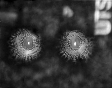
Title: The Eyes of Gollum
Magnification: 1,000X
Instrument: Leitz Wetzlar, the picture was taken with Polaroid Polapan 400 ISO 400/270 film through an Olympus 095442 mounted camera.
Submitted by: Bobb Mohondro, Fusion Semiconductor Systems
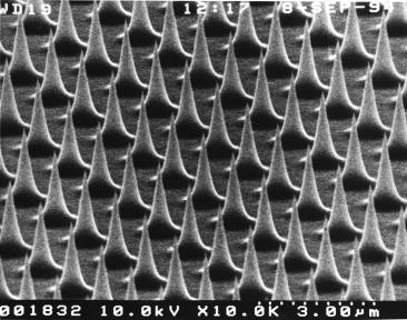
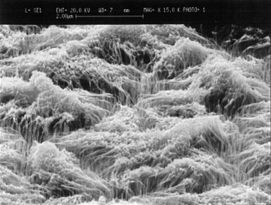
Title: “Nano-Velcro” or “Honey, I think the shag carpet needs vacuuming again.”
Magnification (for 4″ Height): 5,000X
Instrument: JEOL JSM 6400 FX Scanning Electron Microscope
Submitted by: Joel Wendt, Sandia Nantional Laboratories
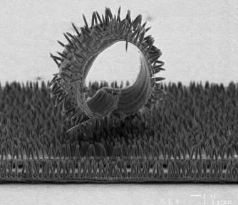
Title: “The Horns of a Dilemna – A Fakir’s Delight”
Magnification (for 4″ image height): 10,000X
Instrument: Hitachi S4000 FE Scanning Electron Microscope
Submitted by: Ezaz Hug and Ron Lawes, Rutherford Appleton Laboratory, ENGLAND
Title: Shortly Before Sunrise in Photonics County
Magnification (for 4″ image height):
Instrument: JEOL 860F Scanning Electron Microscope
Submitted by: Hans Koops Deutch Telecom AG Darmstadt Germany
Title: Broken Sticks
Magnification (for 4″ image height): 3000X
Instrument: Hitachi SEM
Submitted by: Victor White, University of Wisconsin, Madison
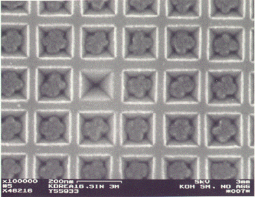
Title: Storm in Micropacific: Silicon Waves
Magnification (for 4″ image height): 11400X
Instrument: BS-300 Tesla, Scanning Electron Microscope.
Submitted by: Sergey Babin, Etec Systems Inc.
Title: Shark Attack
Magnification (for 4″ image height): 6500X
Instrument: FEI DP 620
Submitted by: G. David Via, USAF Wright Laboratory
Title: Pillar Bridges
Magnification (for 4″ image height):
Instrument: Philips XL-40 FEG Scanning Electron Microscope
Submitted by: Martin Verheijen and Frans Holthuysen, Philips Research Eindhoven
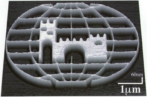
Title: Jerusalem of Gold
Magnification (for 4″ image height):
Instrument: Topometrix TMX 2010 AFM
Submitted by: Dr. Diana Mahalu and Dr. Sidney Cohen, Weizmann Institue of Science, Rehovot, Israel
Title: Amber fields of GaN
Magnification (for 4″ image height): 15,000X
Instrument: Cambridge 5360 Scanning Electron Microscope
Submitted by: Ilesamni Adesida and Chris Youtsey, University of Illinois
Title: Mystery of the Missing Mushroom
Magnification (for 4″ image height): 100,000X
Instrument: LEO 982 Scanning Electorn Microscope
Submitted by: Andrea Franke, MIT
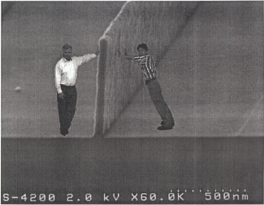
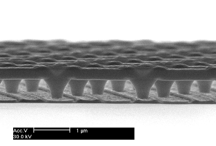
Title: How we get those skinny lines to stand up.
Magnification (for 4″ image height):
Instrument: Scanning Electron Microscope
Submitted by: John Bjorkholm and Joe Langston INTEL
NOTE: This micrograph is clearly in violation of the rules (multiple images) and was not eligible for an official award. However, the judges loved it and it was awarded this honorlable mention.