←1995 |
1997→ |
Ion and Photon Beam Technology and NanofabricationBizarre/Beautiful Micrograph Contest
“A good Micrograph is worth more than the MegaByte it consumes.”
Results Submitted by John Randall
- Best Electron Micrograph
- Best Ion Micrograph
- Best Photon Micrograph
- Best Scanning Probe Micrograph
- Most Bizarre
- Grand Prize
The rules included the following:
- Contestants must be registered 1996 conference attendees.
- Micrographs must be submitted as an 8 inch by 10 inch and must be accompanied by a completed entry sheet.
- Entries must be of a single image taken with a microscope and may not be significantly altered.
- There is no restriction with respect to the subject matter.
- Electron and ion micrographs must be black and white.
Over 40 entries were submitted. There were many outstanding micrographs. The work represented in the submitted micrographs covered a wide range of fields including micro mechanical and integrated circuit fabrication, chemical and dry etching, field emission tips, UV and x-ray optics, and of course e-beam, ion beam, x-ray, and photo lithography experiments. While the largest number of entries were electron micrographs, the grand prize winner was an optical micrograph (ironically of an e-beam experiment). Although there was a small number of scanning probe micrograph entries, the judges chose not to award a prize in that category. The panel of judges who selected the award winners consisted of:
Al Wagner
Research Staff Member, IBM Research
Evelyn Hu
Director of Quest, University of California at Santa Barbara.
Yasuo Iida
Research and Operational Planning Manager, Microelectronics Research Laboratories, NEC Corporation
Visitor count: accesses since June, 1997.
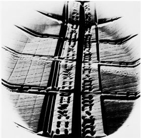
Title: Memory Town
Magnification: 50X
Instrument: Philips 525M Scanning Electron Microscope
Submitted by: Martin Verheijen and Frans Holthuysen, Philips Research, Eindhoven, The Netherlands
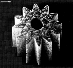
Title: MEMS fabricated Ni Sprocket
Magnification: 1,000X
Instrument: FEI FIB 610
Submitted by: Terrence Stark, Analytical Instrumentation Facility, North Carolina State University
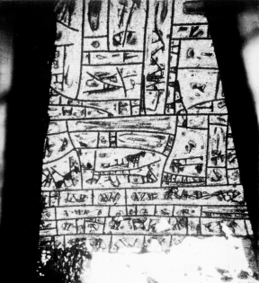
Title: “Hieroglyphics of porous silicon”
Magnification: 50X
Instrument: Olympus
Submitted by: M. Vaez-Iravani, J.K. Rogers, and F.J. Seiferth. Rochester Institute of Technology. M. Vaez-Iravani presently with Tencor Instruments.
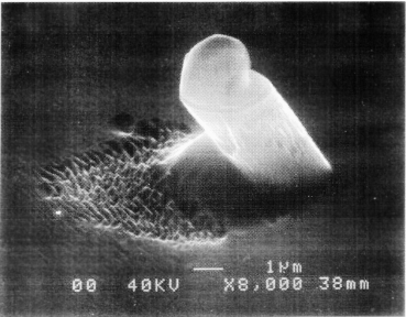
Title: “Micro Duck”
Magnification: 8,000X
Instrument: JEOL 6400
Submitted by: Chuan-Cheng Cheng, California Institute of Technology
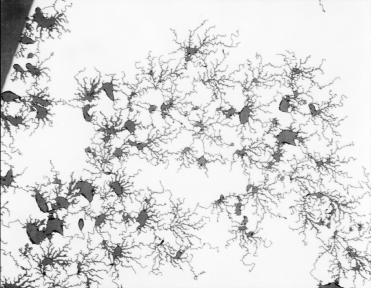
Title: Nervous Breakdown
Magnification: 200X
Instrument: Leitz Ergolux
Submitted by: Tom Newman – Ultratech Stepper, Mark McCord – Stanford University, and Fritz Hohn – IBM Research.